Voices of Industry Channel

It takes a community of embedded designers to develop the myriad applications that are newly available each day. This series gives voice to the members of the embedded design community as they share their experiences and knowledge in their expert application domains so that designers in other application domains can benefit from their lessons learned.

Boosting energy efficiency – How microcontrollers need to evolve

Monday, February 21st, 2011 by Oyvind Janbu

Whatever the end product, all designers have specific tasks to solve and their solutions will be influenced by the resources that are available and the constraints of cost, time, physical size and technology choice.  At the heart of many a good product, the ubiquitous microcontroller often has a crucial influence on system power design and particularly in a brave new world that’s concerned with energy efficiency, users are entitled to demand a greater service from them.  The way microcontrollers are built and operate needs to evolve dramatically if it is to achieve the best possible performance from limited battery resources.

Bearing in mind that the cost of even a typical coin cell battery can be relatively high compared to that of a microcontroller, there are obvious advantages in designing a system that offers the best possible energy efficiency.  It can enable designers to reduce the cost and size of a battery.  Secondly, it can enable designers to significantly extend the lifetime of a battery, consequently reducing the frequency of battery replacement and for certain products the frequency, cost and ‘carbon footprint’ associated with product maintenance call-outs.

Microcontrollers, like many other breeds of electronic components, are these days very keen to stress their ‘ultra low power’ credentials, which is perfectly fine and appropriate where a device’s dynamic performance merits; however, with a finite amount of charge available from a battery cell, it is how a microcontroller uses energy (i.e. power over the full extent of time), that needs to be more closely borne in mind.
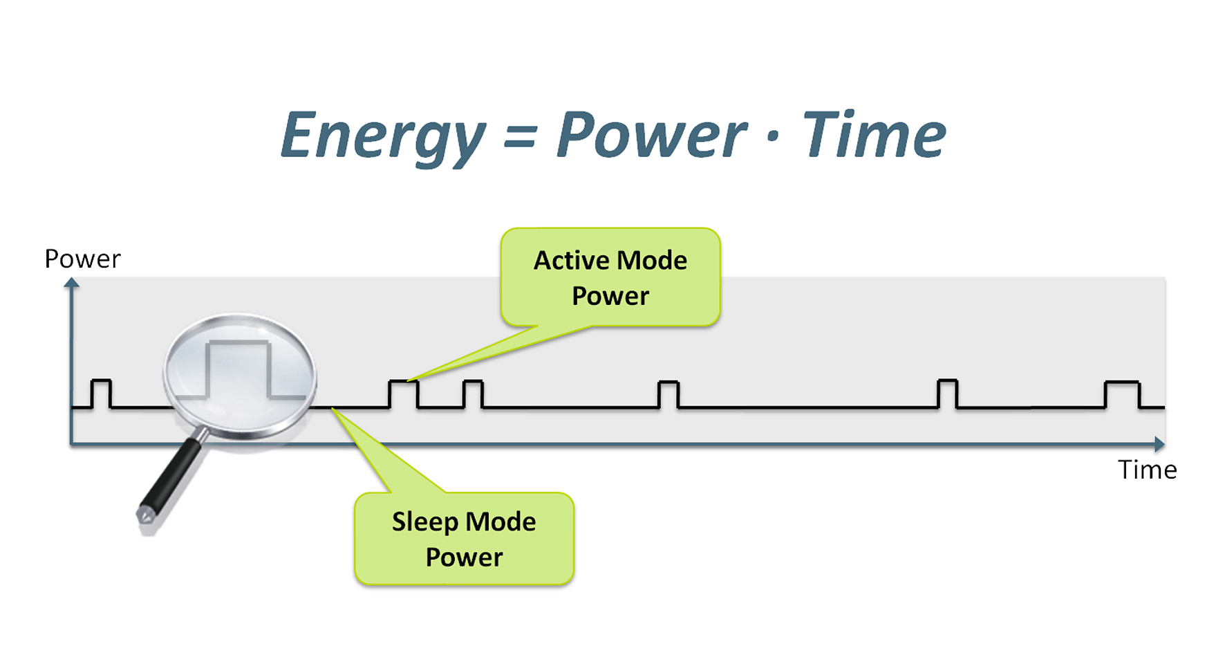
Microcontroller applications improve their energy efficiency by operating in several states – most notably active and sleep modes that consume different amounts of energy.

Product designers need to minimize the product of current and time over all phases of microcontroller operation, throughout both active and sleep periods (Figure 1). Not only does every microamp count, but so does every microsecond that every function takes.  This relationship between amperage and time makes the comparison of 8-, and 16-bit microcontrollers with 32-bit microcontrollers less straightforward. Considering alone their current consumption characteristics in a deep-sleep mode, it is easy to understand why 8-bit or 16-bit microcontrollers have been in an attractive position in energy sensitive applications, where microcontroller duty cycles can be very low.  A microcontroller may after all stay in a deep sleep state for perhaps 99% of the time.

However, if product designers are concerned with every microamp and microsecond every function takes, then using a 32-bit microcontroller should be being considered for even in the ‘simplest’ of product designs.  The higher performance of 32-bit processors enables the microcontroller to finish tasks quicker so that they can spend more time in the low-power sleep modes, which lowers overall energy consumption.  32-bit microcontrollers are therefore not necessarily ‘application overkill’.

More than that though, even simple operations on 8-bit or 16-bit variables can need the services of a 32-bit processor if system energy usage goals are to be achieved.  By harnessing the full array of low-power design techniques available today, 32-bit cores can offer a variety of low-power modes with rapid wake-up times that areon par with 8-bit microcontrollers.

There is a common misconception that switching from an 8-bit microcontroller to a 32-bit microcontroller will result in bigger code size, which directly affects the cost and power consumption of end products.  This is borne of the fact that many people have the impression that 8-bit microcontrollers use 8-bit instructions and 32-bit microcontrollers use 32-bit instructions.  In reality, many instructions in 8-bit microcontrollers are 16-bit or 24-bit in length.

The ARM Cortex-M3 and Cortex-M0 processors are based on the Thumb-2 technology, which provides excellent code density.  Thumb-2 microcontrollers have 16-bit as well as 32-bit instructions, with the 32-bit instruction functionality a superset of the 16-bit version.  Typical output from a C compiler gives 90% 16-bit instructions. The 32-bit version would only be used when the operation cannot be performed with a 16-bit instruction.  As a result, most of the instructions in an ARM Cortex microcontroller program are 16-bits.  That’s smaller than many of the instructions in 8-bit microcontrollers, typically providing less compiled code from a 32-bit processor than 8- or 16-bit microcontrollers.

The second part in this three part series looks deeper at the issues around microcontroller sleep modes.

Energy Management in Power Architecture

Tuesday, December 21st, 2010 by Fawzi Behmann

Embedded computing applications, such as printers, storage, networking infrastructure and data center equipment, continue to face the challenge of delivering increased performance within a constrained energy budget. In February 2009, the Power architecture added power management features in the Power ISA v.2.06 (the most recent specification). The largest gains in performance while maintaining a constrained energy budget comes from creating systems that can pace the workload with energy consumption in an intelligent and efficient manner.

In general, the work performed in embedded computing applications is done in cycles – a combination of active states, management states, and dormant states – and that different areas of the system may have higher demand for energy than other areas throughout the workflow. It becomes important for system architects to model the system from an energy consumption perspective and employing energy saving techniques to the building blocks (CPUs, ASICs and I/Os) of their computing system.

The processor is the heart of the system.  There will be times when high frequencies will be required, but these will likely be very short cycles in the work flow. The vast majority of time, the processor is being asked to perform relatively low-performance tasks. Reducing the processor’s clock frequency during these management periods saves energy, which in turn be used by the ASIC or I/O that are working harder. Throughout the workflow, energy demands vary among system components. Some devices need more power than others, and the system needs to tightly control and manage the power sharing. It is also important that software saves previous known states in non-volatile memory so that the processor can retrieve those states upon entering a more active state.

In many applications, high computing performance during periods of activity should be balanced with low power consumption when there is less workload. Microprocessor cores typically operate at higher frequencies than the rest of the system. Therefore, power consumption can be best minimized by controlling core frequency.  Software can dynamically increase or decrease the core’s clock frequency while still allowing the rest of the system continues operating at the previous frequency.

The Power ISA v.2.06 includes specifications for hypervisor and virtualization on single and multi-core processor implementations. The Power Architecture includes support for dynamic energy management; some of which are enabled internally in the core. For example, it is common for execution units in the processor pipeline to be power-gated when idle. Furthermore, Power Architecture cores offer software-selectable power-saving modes. These power-saving modes reduce the function available in other areas, such as limiting cache and bus-snooping operations, and some modes turn off all functional units except for interrupts. These techniques are effective because they reduce switching on the chip and give operating systems a means to exercise dynamic power management.

Sometimes only the application software running on the processor has the knowledge required to decide how power can be managed without affecting performance. The Power ISA 2.06 added the wait instruction to provide application software with a means to optimize power by enabling the application software to initiate power savings when it is known that there is no work to do until the next interrupt. This instruction enables power savings through user-mode code, and it is well matched to the requirements of the LTE market segment, which requires that the total SoC power be managed effectively. The combination of CPU power-savings modes, the wait instruction, and the ability to wake on an interrupt has been demonstrated to achieve deep sleep power savings with wake up on external events.

To Design Innovative Products, You Must Fail Quickly.

Friday, November 12th, 2010 by Casey Weltzin

While making incremental changes to existing embedded designs may be straightforward, engineers and scientists working on creating new, innovative designs live in a much different world. They are tasked with building complex electrical or electro-mechanical systems that require unique combinations of I/O and processing elements to build. Rather than starting by budgeting time and resources, these designers often need to begin the design process by asking “is this even possible?”

One example of this kind of innovative application is a system created by KCBioMedix, which teaches premature infants how to feed. With up to one-third of premature infants born in the United States suffering from feeding problems, the device called NTrainer, helps coordinate sucking, swallowing, and breathing movements to accelerate feeding without a tube. It is essentially a computerized pacifier that emits gentle pulses of air into an infant’s mouth.

Of course, this kind of innovation seldom takes place without skeptics. Innovative designs require investment that is often heavily competed for and scrutinized within organizations. Or, in the case of startup ventures, entrepreneurs require investment from venture capitalists that have many other places to put their funding. Ultimately, to make a commitment, management or third party sources of capital require the same things – proof that the concept will work and a sound business plan.

Let’s concentrate on the former. Complex devices and machines typically require tens or even hundreds of iterations during the design process; in short, failures. And these iterations can be time consuming and expensive. While making software modifications is relatively easy, changing I/O or processing hardware can take weeks to months. Meanwhile, business leaders and investors become increasingly impatient.

How can both large organizations and startups mitigate the risk of redesigns? One solution commonly employed is to carefully study design requirements and come up with an architecture that is unlikely to need modification. This is a poor solution for two reasons. First, even the most capable designers may fail to foresee the challenges associated with a new, innovative design – resulting in cut traces or a rat’s nest of soldered wires to modify a piece of hardware. Second, because engineers are likely to reuse the architectural patterns and design tools they are used to, innovative features are more likely to be traded-off to fit the constraints that those patterns impose.

A better solution is to use a COTS (commercial off-the-shelf) prototyping platform with a combination of modular I/O, reconfigurable hardware, such as FPGAs (field programmable gate arrays), and high-level development tools. Using this approach, extra I/O points can be “snapped-in” when needed rather than requiring an entire board or daughterboard redesign. Additionally, FPGAs enable designers to implement high-performance custom logic at several orders of magnitude less upfront cost than ASICs (application-specific integrated circuits). Finally, high-level design tools enable both experienced embedded designers and application experts to take advantage of FPGA, real-time operating system, and other technologies without prior expertise or a large team of experts in each technology. In other words, when equipped with the right tools, a small team can “fail quickly” and accelerate the innovation process.

There are a number of economic concerns that must be addressed when using COTS platforms for prototyping. First, since these platforms typically present a much higher up-front cost compared to the BOM (bill of material) components used in a final design, organizations must carefully consider the productivity savings they provide to determine the time to break-even on the investment. For many complex projects, COTS solutions have the potential to reduce the time to first prototype by weeks or months while also reducing the overall size of the development team required. And, it may be possible to reuse these tools between multiple projects in innovation centers (amortizing the upfront cost over a longer period of time).

Another economic consideration that must be made is how much the transition from prototype to final deployment will cost. For small or medium size deployments, it may be beneficial to use COTS hardware embedded in the final device (provided that it meets size and power constraints) – essentially a trade-off between higher BOM cost and reduced development time. On the other hand, for large deployments the benefits of a low BOM cost may warrant moving to a custom cost-optimized design after prototyping. In this case, organizations can save cost by choosing prototyping tools that provide a minimal-investment path to the likely deployment hardware.

Returning to the example of KCBioMedix, the company was able to reduce prototyping time of their premature infant training system from 4 months to 4 weeks using COTS tools – providing an estimated savings of $250,000. COTS hardware is also being used in the final NTrainer product to maximize reuse of IP from the prototyping stage.

The bottom line is that for both the aspiring entrepreneur and the large organization that wishes to maintain an entrepreneurial spirit, prototyping is an essential part of producing innovative designs in time to beat the competition. Organizations that encourage prototyping are more nimble at weeding out good ideas from bad, and ultimately producing differentiated products that command strong margins in the marketplace.

Balancing risk versus innovation – configuration in the design platform

Monday, October 25th, 2010 by Rob Evans

An approach to balance the risk-innovation stalemate is to introduce robust, high-integrity design data management into the electronic design space itself, where it becomes part of the design process, rather than an ‘add-on’ that gets in the way and stifles innovation. This is no trivial task, and needs to be done at the fundamental levels of the design environment, and through all domains. It starts by changing the way the design environment models the process from a collection of disconnected design ‘silos’, to a single concept of product development. In turn, this effectively creates a singular design platform, with the unified data model representing the system being designed.

A platform-based approach offers the possibility of mapping the design data as a single, coherent entity, which simplifies both the management of design data and the process for generating and handing over the data required for procurement and manufacturing. A singular point of contact then exists for all design data management and access, both inside and outside the design environment.

This approach provides a new layer of configuration management that is implemented into the design environment itself, at a platform level. Along with managing the design data, it allows the creation of formal definitions of the links between the design world and the supply chain that is ultimately responsible for building the actual products.

These definitions can be managed as any number of ‘design configurations’. They map the design data, stored as versions of design documents in a nominated repository (a version-controlled design vault), to specific revisions of production Items (blank and assembled boards) that the supply chain is going to build. This formalized management of design data and configurations allows changes to be made without losing historical tracking, or the definitions of what will be made (a design revision) from that version of the design data.

With the design data and configurations under control at a system level, a controlled (or even automated) design release process can potentially eliminate the risks associated with releasing a design to production. This tightly controlled release process extracts design data directly from the design vault, validates, and verifies it with configurable rule checkers, and then generates the outputs as defined by the link definitions. The generated outputs are pushed into a ‘container’ representing a specific revision of the targeted item (typically a board or assembly) that is stored in a design ’release vault’.

In this way all generated outputs, stored as targeted design revisions, are contain in that centralized storage system, where those released for production (as opposed to prototype or ones that may have been abandoned) are locked down and revisioned. It also facilitates support for a simple lifecycle management process that allows the maturity of the revision’s data to be controlled and defined, as well as providing a high-integrity foundation for integration with PLM and PDM systems for those organizations that use them, or plan to.

Such a system supports high-integrity design data management in a platform that allows for productivity and design innovation. This eliminates manual or externally imposed systems that attempt to control design data integrity, along with their associated restrictions in design flexibility and freedom. This system applies to the management of data within the design space, and perhaps more importantly, to the process of releasing the required outputs through to an organization’s supply chain. In practice, it reduces the risk of going to production with a design that was not validated, not in sync, or consists of an incomplete set of manufacturing data.

With formalized, versioned storage ‘vaults’ (for design and release) the system can provide an audit trail that gives you total visibility from the release data back to the source data, even to the level of hour to hour changes to that design information. This coupled with the unique application of configurations to define the links between a design and the various production items to be made, allows design management to become an inherent part of the product development process – as opposed to a constricting system imposed over the top of design.

But most importantly, design can be undertaken without having to give up the flexibility, freedom and creative innovation that’s needed to create the next generation of unique and competitive product designs.

Balancing risk versus innovation – disconnect between design and production

Monday, October 4th, 2010 by Rob Evans

Risk minimization, particularly at the stage of releasing design data to production and manufacturing, has been the focus of increasing attention as the product development landscape has changed. One of the most significant shifts in the way organizations work manifests in the disconnection between design and manufacturing, where a product is now likely to be manufactured in a completely different location (region or country) from where it is designed. Fuelled by the rise of a truly global electronics industry, outsourcing or ‘offshoring’ manufacture is now commonplace because the potential cost and efficiency benefits are hard to ignore for most organizations.

This change in the product development process has pulled the spotlight firmly on the need to manage and raise the integrity of design data, prior to its release to production and across the entire product development process. Manufacturing documents now need to be sent to fabrication and assembly houses in other parts of the world with different time zones, and possibly languages, which has raised the risk associated with pushing the design release button to a whole new level. You can’t just pop next door to correct a problem during the production stage.

Consequently, there is a strong push for improving both the quality and integrity of the release process, and not surprisingly, an even more rigorous application of the existing design lock-down methodology to minimize risk. In the design space, engineers are forced to adopt more stringent levels of the formalized, locked-down process with the aim of overcoming the much higher risks created by the distance between design and manufacturing. Ultimately, the best and most potentially successful design is wasted effort if poor data integrity causes manufacturing errors, or perhaps worse, if the resulting design respins cause it to be manufactured too late.

The flip side of the risk management coin, promoting design innovation, is the opposing force in current electronics design landscape. While always an important element, the capacity for innovation in electronics design is now crucial to an organization’s success or in some cases its survival. However, every new feature and every product change is a potential source for something to go wrong. We have the crucial need for effective product and feature innovation running headlong into the equally important (and increasing) demand for design control and data integrity.

Companies both large and small now face aggressive competition from all over the world in what has become a globalized electronics industry, and this very environment has opened opportunities for efficient outsourcing. Product individuality and delivering a unique user experience have become the characteristics that define a device’s competitive status amongst the crowd, and those assets can only be sourced though innovation in design.

The need for establishing a clear competitive edge through innovative design, rather than (failing) traditional factors such as price, means that creating the product value and functionality customers are seeking relies on an unrestrained design environment. This freedom allows developers to explore design options, promotes experimentation, and allows for frequent, iterative changes during design exploration. Also, it is a more fulfilling and enjoyable way to design.

The final part of this three part series proposes a different approach to the risk-innovation stalemate.

Balancing risk versus innovation – design data management

Friday, September 17th, 2010 by Rob Evans

Like most creative design processes, electronics design would be whole lot easier without the need to consider the practicalities of the real end result – in this case, a tangible product that someone will buy and use. Timelines, cost limitations, component restrictions, physical constraints, and manufacturability would fade to the background, leaving behind unrestrained design freedom without the disruptive influence of external considerations.

It is a nice thought, but the reality is that electronics design is just one part of the large, complex product design puzzle, and the puzzle pieces are no longer discrete entities that can be considered in isolation. The pieces unavoidably co-influence and interact, which makes the design development path to a final product a necessarily fluid and complex process. It is also one that involves managing and bringing together an increasing number of variable, co-dependent elements – the pieces of the puzzle – from different systems and locations. Pure electronics design is one thing, but successfully developing, producing, and keeping track of a complete electronic product is a much larger story.

From an electronics design perspective, those broader product development considerations are influencing and constraining the design process more than ever before. At the very least, the shift towards more complex and multi-domain electronic designs (typically involving hardware, software, programmable hardware and mechanical design) means a proportional increase in the risk of design-production errors. This has inevitably led to imposing tighter controls on the design process, as a risk management strategy.

From an organization’s point of view there seems little alternative to a risk-minimization approach that is based on tying down the electronics design process to control change. Leave the management of design open and design anarchy, or expensive errors, are likely outcomes. From an overall product development perspective, the peak in the risk-timeline curve (if there is such a thing) tends to be the transition from design to the production stage. This is a one-way step where an error, and there’s plenty to choose from, will delay and add cost to the final product – not to mention missed market opportunities, painful design re-spins and damaged customer relationships.

To increase the integrity of the design data that is released to production, most organizations are managing the electronic product development process by imposing a layer of control over the design process. This aims to control change and can take on a variety of forms, including manual paper-based sign-off procedures as well as external audit and approval systems. The common thread is that these approaches are an inevitable restriction in design freedom – in other words, they impose limits on how and when design changes can be made.

By restricting design experimentation and exploratory change, this ‘locked down’ product development environment does not encourage the design innovation that is crucial to creating competitive products. The upshot is that organizations must now balance two opposing forces when managing the product development process – the need to foster innovation versus the need to manage risk by maintaining design data integrity.

The second part in this three part series explores controlling risk.

Man vs. Machine: What’s behind it?

Friday, September 3rd, 2010 by Binay Bajaj

The interaction between ‘man and the machine’ today is very different when compared to 20 – even 10 – years ago. Major changes include how a person interfaces with his everyday consumer device such as a smart phone, notebook, tablet, or navigational device. In the past, a user might push several mechanical buttons to play a handheld game or control household appliances, whereas now, they can use various touch gestures on a screen to play a handheld game, look up directions on a map, read a book on a tablet, or even control the sound of his stereo from a touchscreen.

There have been a number of devices for many years with enhanced functionality but most of these features were not used because it was too complicated. Easy and intuitive interfaces open up a device for the user. Users can quickly discover the power of the device, finding it interactive and enabling them to spend hours on the device, playing with it, and enhancing it by finding new applications.

So what is behind these devices that include intuitive interfaces? What is required to enable these devices to function with such rich user interfaces? The secret is good touch hardware, firmware, as well as the right algorithm and software drivers. These features are all part of a good touch solution that provides design engineers the tools to add touch functionality to various devices.

Many vendors are not ‘end device’ manufacturers; rather, they make the controller and touch solution for OEMs (original equipment manufacturer). These vendors provide a complete touch system so OEMs can implement a feature-rich, intuitive interface in the device for the users. These touch solutions include the touch controller, firmware, touch sensor pattern design, sensor test specification, manufacturing test specification, and software drivers.

However, the OEM needs to do an evaluation of the touch solution at the time of engagement. This is where a sensor evaluation kit showcases the capability of the solution and how the touch solution matches the customer requirement. A software development kit can provide performance characterization, as well as a development platform environment to support various operating systems. A good development kit is easy-to-understand, easy-to-install, and quick.

The software development kit for touch functionality is a key part of the package because it requires the design engineer to install the package himself. Easy-to-use is the key. The vendor provides the hardware and using it may require some collaboration, but the software development kit is typically the challenge for designers. The types of instructions that a touch development kit needs to provide in order to be easy-to-use include how to set-up the board, how to demonstrate the board’s capabilities, and how to configure the software settings.

Vendors understand that the easier it is to use a development kit, the more robust a design engineer can make a product and bring it to market faster. Software development kits make it apparent that the designer can control these various features to offer more touch functionality to the consumers including software algorithms, gestures, lower power, faster response time, and higher accuracy.

Though the interaction between ‘man and the machine’ is changing today, each year brings unlimited possibilities to the market place. The human interface to devices will continue to become easier and support more intuitive interactions between the man and his machine.

Touchscreen User Interface checklist: criteria for selection

Thursday, August 19th, 2010 by Ville-Veikko Helppi

Touchscreens require more from the UI (user interface) design and development methodologies. To succeed in selecting the right technology, designers should always consider the following important topics.

1) All-inclusive designer toolkit. As the touchscreen changes the UI paradigm, one of the most important aspects of the UI design is how quickly the designer can see the behavior of the UI under development. Ideally, this is achieved when the UI technology contains a design tool that allows the designer to immediately observe behavior of the newly created UI and modify easily before target deployment.

2) Creation of the “wow factor.” It is essential that UI technology enables developers and even end-users to easily create clever little “wow factors” on the touchscreen UI. These technologies, which allow the rapid creation and radical customization of the UI, have a significant impact on the overall user experience.

3) Controlling the BoM (Bill of Material). For UIs, everything is about the look and feel, ease of use, and how well it reveals the capabilities of the device. In some situations, adding a high-resolution screen with a low-end processor is all that’s required to deliver a compelling user experience. Equally important is how the selected UI technology reduces engineering costs related to UI work. Adapting a novel technology that enables the separation of software and UI creation enables greater user experiences without raising the BoM.

4) Code-free customization. Ideally, all visual and interactive aspects of a UI should be configurable without recompiling the software. This can be achieved by providing mechanisms to describe the UI’s characteristics in a declarative way. Such a capability affords rapid customization without any changes to the underlying embedded code base.

5) Open standard multimedia support. In order to enable the rapid integration of any type of multimedia content into a product’s UI (regardless of the target hardware) some form of API standardization must be in place. The OpenMAX standard addresses this need by providing a framework for integrating multimedia software components from different sources, making it easier to exploit silicon-specific features, such as video acceleration.

Just recently, Apple replaced Microsoft as the world’s largest technology company. This is a good example of how a company that produces innovative, user-friendly products with compelling user interfaces can fuel the growth of technology into new areas. Remember, the key isn’t necessarily the touchscreen itself – but the user interfaces running on the touchscreen. Let’s see what the vertical markets can do to take the user interface and touchscreen technology to the next level!

Impacts of touchscreens for embedded software

Thursday, August 5th, 2010 by Ville-Veikko Helppi

No question, all layers of the embedded software are impacted when a touchscreen is used on a device. A serious challenge is finding space to visually show a company’s unique brand identity, as it is the software that runs on the processor that places the pixels on screen. From the software point of view, the touchscreen removes one abstraction level between the user and software. For example, many devices have removed ‘OK’ buttons from dialogs as the user can click the whole dialog instead of clicking the button.

Actually, software plays an even more critical role as we move into a world where the controls on a device are virtual rather than physical. In the lowest level of software, the touchscreen driver provides a mouse-emulation that basically means the same as clicking a mouse cursor on certain pixels. However, the mouse driver gets its data as “relative” while the touchscreen driver gets its data as “absolute.” Writing the touchscreen driver is usually trivial, as this component only takes care of passing information from the physical screen to higher levels of software. The only inputs the driver needs are Boolean if the screen is touched, and in what x- and y-axes has the touch taken place.

At the operating system level, a touchscreen user interface means more frequent operating system events than the typical icon or widget-based user interface. In addition to a touchscreen, there may also be a variety of different sensors (e.g., accelerometers) inputting stimuli to the operating system through their drivers. Generally, the standardized operating system can give confidence and consistency to device creation, but if it needs to be changed, the cost of doing so can be astronomical due to testing the compatibility of other components.

The next layer is where the middleware components of the operating system are found, or in this context, where the OpenGL/ES library performs. Various components within this library do different things from processing the raw data with mathematical algorithms, providing a set of APIs for drawing, interfacing between software and hardware acceleration, or providing services such as rendering, font engines, and so on. While this type of standardization is generally a good thing, in some cases, it can lead to non-differentiation – in the worst case, it might even kill the inspiration of an innovative user interface creation. Ideally, the standardized open library, together with rich and easily customizable user interface technology, results in superb results.

The application layer is the most visible part of the software and forms the user experience. It is here where developers must ask:

1)      Should the application run in the full-screen mode or enable using widgets distributed around the screen?

2)      What colors, themes, and templates are the best ways to illustrate the behavior of the user interface?

3)      How small or large should the user interface elements be?

4)      In what ways will the user interface elements behave and interact?

5)      How intuitive do I want to make this application?

Compelling UI design tools is essential for the rapid creation of user interfaces.

In the consumer space, there are increasingly more competitive brands with many of the same products and product attributes. Manufacturers are hard-pressed to find any key differentiator among this sea of “me too” offerings. One way to stand out is by delivering a rich UI experience via a touchscreen display.

We are starting to see this realization play out in all types of consumer goods, even in white goods as pedestrian as washing machines. There are now innovative display technologies replacing physical buttons and levers. Imagine a fairly standard washing machine with a state-of-the-art LCD panel. This would allow the user to easily browse and navigate all the functions on that washing machine – and perhaps learn a new feature or two. By building an attractive touchscreen display, simply changing the software running on the display can manifest any customization work. Therefore, things like changing the branding, adding compelling video clips and company logos, all become much simpler because it’s all driven by software. If the manufacturer uses the right technology, they may not even need to modify the software to change the user experience.

Driven by the mobile phone explosion, the price point of display technology has come down significantly. As a result, washing machine manufacturers can add more perceived value to their product without necessarily adding too much to the BoM (bill of materials). Thus, before the machine leaves the factory, a display technology may increase the BoM by $30, but this could increase the MSRP by at least $100. No doubt, this can have a huge impact on the company’s bottom line. This results in a “win-win” for the manufacturer and for the consumer. The manufacturer is able to differentiate the product more easily and in a more cost effective manner, while the product is easier to use with a more enhanced UI.

The final part in this four-part series presents a checklist for touchscreen projects.

The User Interface Paradigm Shift

Thursday, July 22nd, 2010 by Ville-Veikko Helppi

Touchscreens are quickly changing the world around us. When clicking on an image, a touchscreen requires much less thinking and more user intuition. Touchscreens are also said to be the fastest pointing method available, but that isn’t necessarily true – it all depends on how the user interface is structured. For example, most users accept a ten millisecond delay when scrolling with cursor and mouse, but with touchscreens, this same period of time feels much longer so the user experience is perceived as not as smooth. Also, multi-touch capabilities are not possible with mouse emulations, at least, not as intuitively as with a touchscreen. The industry has done a good job providing a screen pen or stylus to assist the user when selecting the right object on smaller screens, thus silencing the critics of touchscreens who say it’s far from ideal as a precise pointing method.

The touchscreen has changed the nature of UI (user interface) element transitions. When looking at motions of different UI elements, these transitions can make a difference in device differentiation and if implemented properly tell a compelling story. Every UI element transition must have a purpose and context as it usually reinforces the UI elements. Something as simple as buffers are effective at giving a sense of weight to a UI element – and moving these types of elements without a touchscreen would be awkward. For UI creation, the best user experience can be achieved when UI element transitions are natural and consistent with other UI components (e.g., widgets, icons, menus) and deliver a solid, tangible feel of that UI. Also, the 3D effects during the motion provide a far better user experience.

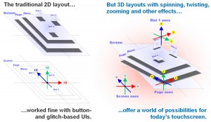
3D layouts enable more touchscreen friendly user interfaces.

Recent studies in human behavior along with documented consumer experiences have indicated that the gestures of modern touchscreens have expanded the ways users can control a device through its UI. As we have seen with “iPhone phenomena” the multi-touchscreen changes the reality behind the display screen, allowing new ways to control the device through hand-eye (e.g., pinching, zooming, rotating) coordination. But it’s not just the iPhone that’s driving this change. We’re seeing other consumer products trending towards simplifying the user experience and enhancing personal interaction. In fact, e-Books are perfect examples. Many of these devices have a touchscreen UI where the user interacts with the device directly at an almost subconscious level. This shift in improved user experience has also introduced the idea that touchscreens have reduced the number of user inputs required for the basic functioning of a device.

The third part in this four-part series explores the impact of touchscreens on embedded software.