Balancing risk versus innovation – disconnect between design and production

Monday, October 4th, 2010 by Rob Evans

Risk minimization, particularly at the stage of releasing design data to production and manufacturing, has been the focus of increasing attention as the product development landscape has changed. One of the most significant shifts in the way organizations work manifests in the disconnection between design and manufacturing, where a product is now likely to be manufactured in a completely different location (region or country) from where it is designed. Fuelled by the rise of a truly global electronics industry, outsourcing or ‘offshoring’ manufacture is now commonplace because the potential cost and efficiency benefits are hard to ignore for most organizations.

This change in the product development process has pulled the spotlight firmly on the need to manage and raise the integrity of design data, prior to its release to production and across the entire product development process. Manufacturing documents now need to be sent to fabrication and assembly houses in other parts of the world with different time zones, and possibly languages, which has raised the risk associated with pushing the design release button to a whole new level. You can’t just pop next door to correct a problem during the production stage.

Consequently, there is a strong push for improving both the quality and integrity of the release process, and not surprisingly, an even more rigorous application of the existing design lock-down methodology to minimize risk. In the design space, engineers are forced to adopt more stringent levels of the formalized, locked-down process with the aim of overcoming the much higher risks created by the distance between design and manufacturing. Ultimately, the best and most potentially successful design is wasted effort if poor data integrity causes manufacturing errors, or perhaps worse, if the resulting design respins cause it to be manufactured too late.

The flip side of the risk management coin, promoting design innovation, is the opposing force in current electronics design landscape. While always an important element, the capacity for innovation in electronics design is now crucial to an organization’s success or in some cases its survival. However, every new feature and every product change is a potential source for something to go wrong. We have the crucial need for effective product and feature innovation running headlong into the equally important (and increasing) demand for design control and data integrity.

Companies both large and small now face aggressive competition from all over the world in what has become a globalized electronics industry, and this very environment has opened opportunities for efficient outsourcing. Product individuality and delivering a unique user experience have become the characteristics that define a device’s competitive status amongst the crowd, and those assets can only be sourced though innovation in design.

The need for establishing a clear competitive edge through innovative design, rather than (failing) traditional factors such as price, means that creating the product value and functionality customers are seeking relies on an unrestrained design environment. This freedom allows developers to explore design options, promotes experimentation, and allows for frequent, iterative changes during design exploration. Also, it is a more fulfilling and enjoyable way to design.

The final part of this three part series proposes a different approach to the risk-innovation stalemate.

When and how much should embedded developers implement robust defenses against malicious software in their designs?

Wednesday, September 29th, 2010 by Robert Cravotta

It is easy to believe that malware, malicious software designed to secretly access a system without the owner’s informed consent, only affects computers. However, as more devices support connection with other devices through a USB port, malware is able to hide and launch itself from all types of devices. For example, earlier this year, Olympus shipped over 1700 units of their Stylus Tough 6010 digital compact camera with an unexpected bonus – the camera’s internal memory was carrying an autorun worm that could infect a user’s Windows computer when they connected the camera to it.

Another example of malware using a USB device as a transport and infection mechanism involves USB sticks that IBM handed out at this year’s AusCERT (Australian Computer Emergency Response Team) conference on the Gold Coast, Queensland. In this case, the USB carried two pieces of malware and was handed out at a conference that focuses on Information Security.

Researchers at Stanford’s Computer Security Lab identify that many low cost devices, such as webcams, printers, and other devices that ship with embedded web interfaces, are not designed to withstand malware attacks despite interfacing with the most sensitive parts of a computer network. According to the researchers, NAS (network-attached storage) devices pose the highest risk because they are susceptible to all five of the attack classes the researchers considered in their study.

There are other examples of companies selling infected end products to users. My key concern is that so many devices are sold at such low margins already that it is unlikely the designs include much attention to withstanding malicious software planting themselves in those devices.

The question is, how much energy and attention should embedded designers give to hardening their designs to stopping malicious software – or being an unintended transport for malicious software? I’m not sure an isolated incident that involves using an infected test computer (such as the Olympus example), which infects the end products during the test, is a basis for changing the design flow other than to ensure the test equipment is not itself infected. How would you, or do you, determine how much effort to put into your embedded design to address malicious software from using your system in an unintended fashion?

The Express Traffic Lane (It’s Not the Computer, It’s How You Use It)

Friday, September 24th, 2010 by Max Baron

Less than a week ago, a section of the diamond lane in California’s southbound Interstate 680 freeway became sensor-controlled or camera-computerized. A diamond lane, for those of us not familiar with the term, is an express traffic lane allowed only to high-occupancy automobiles or types of vehicles that use environmentally friendly fuels or less gasoline.

Also known as the carpool lane, the diamond lane is usually marked by white rhombuses (diamonds) painted on the asphalt to warn solo drivers that they are not allowed to use it. The diamond lane provides fast free commuting for carpoolers, motorcyclists and diamond lane sticker owners. Solo drivers must use the remaining lanes that are usually slower during periods of peak traffic. These single drivers however, are now allowed to use a section of the diamond lane in California’s southbound Interstate 680 freeway — but they have to pay for it.

The camera-computerized or sensor-activated system introduced just a few days ago doesn’t make sense considering the state-of-art of available technology.

Here is how the complex system works. An automobile carrying only its driver must have a FasTrak transponder allowing a California-designated road authority to charge a fee for using this newly created toll-diamond lane. Mounted on a car’s windshield, the FasTrak transponder uses RFID technology to read the data required to subtract the passage fee from the car owner’s prepaid debit account. The fee reflects the traffic level and is changed according to the time of day. The fee is displayed on pole-mounted digital displays.

To avoid being charged if there are also passengers in the automobile, a FasTrak transponder owner must remove the vehicle’s transponder from the car’s windshield. Caught by traffic enforcement (California Highway Patrol) a solo driver without a FasTrak transponder is fined for using the diamond lane without paying for the privilege. Other schemes implemented for instance at a toll plaza, will trigger a camera to take a photo of the delinquent vehicle and its license plate following which a violation notice will be sent to the registered owner of the vehicle.

Considering the complexity of the system from the viewpoint of existing digital cameras, embedded computers, cellular telephony and the presence of police enforcement on the freeway, one can wonder about the necessity of FasTrak devices or police involvement. 

If we are to follow descriptions found on publications such as San Jose’s Mercury daily newspaper (reference) and the freeway’s information brochure (reference), the system seems to be unnecessarily disconnected: an RFID tag is used to pay for solo driving, but police has to check if a vehicle without a transponder is occupied by just the driver or by additional people. If a FasTrak-less driver is detected police must stop the delinquent car and write a ticket. Based on the description, it may seem that the cameras or sensors implemented are unable to differentiate among illegal solo drivers vs. multiple passenger cars. If true, these cameras or sensors are using technology that was state of the art in the 90’s.  They only seem to be able to detect a large object well-enough to report to police the number of vehicles using the lane without transponders, leaving the rest to law enforcement.

Today’s embedded computers equipped with simple cameras can read numbers and words. FasTrak transponders should not be required. Existing systems can identify human shapes and features in cars well enough to differentiate among multiple vs. solo drivers and with adequate software and illumination, they can continue to function correctly despite most adverse weather changes or light conditions. The word “CARPOOL” written by the driver of a multiple-person car can be displayed for the computer to read to ensure that the system will not charge for the use of the toll-lane. The license plate of the solo driver automobile can be linked in a data base to a debit account or to the name and address of the owner.

We estimate the price of a pole-mounted low-power system of this kind including wireless communication at a pessimistic $9,800 as follows: a ruggedized camera– $1,500; a video road image recognition engine plus software such as designed by Renesas for automobiles — $2,000 including software (reference); a controlling embedded computer including a real-time OS — $900; a wireless communication block — $600; components for remote testing, upgrades and servicing–$1,000; battery and power supply– $1,000; solar panels if required–$800; enclosure–$2,000.

In a modern system there would be no fines—just charges made to driver bank accounts if so elected–or monthly statements to be paid along with electrical, gas, and other services for which monthly payments have found acceptance. But, have we been told everything? Do we really know what types of systems are looking today at the traffic on freeway 680’s toll-enabled express lane? This may be just step one.

What are your criteria for when to use fixed-point versus floating-point arithmetic in your embedded design?

Wednesday, September 22nd, 2010 by Robert Cravotta

The trade-offs between using fixed-point versus floating-point arithmetic in embedded designs continues to evolve. One set of trades-offs between using either type of arithmetic involves system cost, processing performance, and ease-of-use. Implementing fixed-point arithmetic is more complicated than using floating-point arithmetic on a processor with a floating-point unit. The extra complexity of determining scaling factors for fixed-point arithmetic and accommodating precision loss and overflow, has historically been offset by allowing the system to run on a cheaper processor, and depending on the application, at lower energy consumption and more accuracy than with a processor with an integrated floating-point unit.

However, the cost of on-chip floating-point units has been dropping for years and they crossed a cost threshold over the last few years as signaled by the growing number of processors that include an integrated floating-point unit (more than 20% of the processors listed in the Embedded Processing Directory device tables now include or support floating-point units). In conversations with processor vendors, they have shared with me that they have experienced more success with new floating-point devices than they anticipated, and this larger than expected success has spurred them to plan even more devices with floating-point support.

Please share your decision criteria for when to use fixed-point and/or floating-point arithmetic in your embedded designs. What are the largest drivers for your decision? When does the application volume make the cost difference between two processors drive the decision? Does the energy consumption between the two implementations ever drive a decision one way or the other? Do you use floating-point devices to help you get to market quickly and then migrate to a fixed-point implementation as you ramp up your volumes? As you can see, the characteristics of your application can drive the decision in many ways, so please share what you can about the applications with which you have experience performing this type of trade.

Alternative touch interfaces – sensor fusion

Tuesday, September 21st, 2010 by Robert Cravotta

While trying to uncover and highlight different technologies that embedded developers can tap into to create innovative touch interfaces, Andrew commented on e-field technology and pointed to Freescale’s sensors. While exploring proximity sensing for touch applications, I realized that accelerometers represent yet another alternative sensing technology (versus capacitive touch) that can impact how a user can interact with a device. The most obvious examples of this are devices, such as a growing number of smart phones and tablets, which are able to detect their orientation to the ground and rotate the information they are displaying. This type of sensitivity enables interface developers to consider broader gestures that involve manipulating the end device, such as shaking it, to indicate some type of change in context.

Wacom’s Bamboo Touch graphic tablet for consumers presents another example of e-field proximity sensing combined with capacitive touch sensing. In this case, the user can use the sensing surface with an e-field optimized stylus or they can use their finger directly on the surface. The tablet controller detects which type of sensing it should use without requiring the user to explicitly switch between the two sensing technologies. This type of combined technology is finding its way into tablet computers.

I predict the market will see more examples of end devices that seamlessly combine different types of sensing technologies in the same interface space. The different sensing modules working together will enable the device to infer more about the user’s intention, which will in turn, enable the device to better learn and adapt to each user’s interface preferences. To accomplish this, devices will need even more “invisible” processing and database capabilities that allow these devices to be smarter than previous devices.

While not quite ready for production designs, the recent machine touch demonstrations from the Berkeley and Stanford research teams suggest that future devices might even be able to infer user intent by how the user is holding the device – including how firmly or lightly they are gripping or pressing on it. These demonstrations suggest that we will be able to make machines that are able to discern differences in pressure comparable to humans. What is not clear is whether each of these technologies will be able to detect surface textures.

By combining, or fusing, different sensing technologies together, along with in-device databases, devices may be able to start recognizing real world objects – similar to the Microsoft Surface. It is becoming within our grasp for devices to start recognizing each other without requiring explicit electronic data streams flowing between those devices.

Do you know of other sensing technologies that developers can combine together to enable smarter devices that learn how their user communicates rather than requiring the user to learn how to communicate with the device?

Balancing risk versus innovation – design data management

Friday, September 17th, 2010 by Rob Evans

Like most creative design processes, electronics design would be whole lot easier without the need to consider the practicalities of the real end result – in this case, a tangible product that someone will buy and use. Timelines, cost limitations, component restrictions, physical constraints, and manufacturability would fade to the background, leaving behind unrestrained design freedom without the disruptive influence of external considerations.

It is a nice thought, but the reality is that electronics design is just one part of the large, complex product design puzzle, and the puzzle pieces are no longer discrete entities that can be considered in isolation. The pieces unavoidably co-influence and interact, which makes the design development path to a final product a necessarily fluid and complex process. It is also one that involves managing and bringing together an increasing number of variable, co-dependent elements – the pieces of the puzzle – from different systems and locations. Pure electronics design is one thing, but successfully developing, producing, and keeping track of a complete electronic product is a much larger story.

From an electronics design perspective, those broader product development considerations are influencing and constraining the design process more than ever before. At the very least, the shift towards more complex and multi-domain electronic designs (typically involving hardware, software, programmable hardware and mechanical design) means a proportional increase in the risk of design-production errors. This has inevitably led to imposing tighter controls on the design process, as a risk management strategy.

From an organization’s point of view there seems little alternative to a risk-minimization approach that is based on tying down the electronics design process to control change. Leave the management of design open and design anarchy, or expensive errors, are likely outcomes. From an overall product development perspective, the peak in the risk-timeline curve (if there is such a thing) tends to be the transition from design to the production stage. This is a one-way step where an error, and there’s plenty to choose from, will delay and add cost to the final product – not to mention missed market opportunities, painful design re-spins and damaged customer relationships.

To increase the integrity of the design data that is released to production, most organizations are managing the electronic product development process by imposing a layer of control over the design process. This aims to control change and can take on a variety of forms, including manual paper-based sign-off procedures as well as external audit and approval systems. The common thread is that these approaches are an inevitable restriction in design freedom – in other words, they impose limits on how and when design changes can be made.

By restricting design experimentation and exploratory change, this ‘locked down’ product development environment does not encourage the design innovation that is crucial to creating competitive products. The upshot is that organizations must now balance two opposing forces when managing the product development process – the need to foster innovation versus the need to manage risk by maintaining design data integrity.

The second part in this three part series explores controlling risk.

What are good examples of how innovative platforms are supporting incremental migration?

Wednesday, September 15th, 2010 by Robert Cravotta

Companies are regularly offering new and innovative processing platforms and functions in their software development tools. One of the biggest challenges I see for bringing new and innovative capabilities to market is supporting incremental adoption and migration. Sometimes the innovative approach for solving a set of problems requires a completely different way of attacking the problem and, as a result, it requires developers to rebuild their entire system from scratch. Requiring developers to discard their legacy development and tools in order to leverage the innovative offering is a red flag that the offering may have trouble gaining acceptance by the engineering community.

I have shared this concern with several companies that brought out multicore or many-core systems over the past few years because their value proposition did not support incremental migration. They required the developer to completely reorganize their system software from scratch in order to fully take advantage of their innovative architecture. In many cases, this level of reorganizing a design represents an extremely high level of risk compared to the potential benefit of the new approach. If a development team could choose to migrate a smaller portion of their legacy design to the new approach and successfully release it in the next version of the product, they could build their experience with the new approach and gradually adopt the “better” approach without taking a risk that was larger than their comfort level.

Based on stories from several software development companies, software development tools are another area of opportunity for new capabilities to benefit from being able to support incremental adoption. In this case though, the new capabilities do not require a redesign, but they require the developer to accept an unknown learning curve to even evaluate the new feature. As the common storyline goes, the software tool vendor has found that describing the new capability, describing how to use it, and getting the developer to understand how that new capability benefits them is not as straight forward as they would like. As a result, some of the newest features they have added to their products go largely unnoticed and unused by their user base. Their frustration is obvious when they share these stories – especially when they talk about the circumstances where developers do adopt the new features. In many cases, a developer calls them with a problem and the software tool vendor explains how they have a capability already in the tool that will help the developer solve that problem. Only then does the developer try out the feature and then adopt using it in future projects, but they had to experience the type of problem that the feature was designed to assist with before they even recognized that the feature was already added to the tool suite.

Rather than harp on the failures of accommodating incremental migration or easing the adoption learning curve, I would like to uncover examples and ideas of how new innovations can support incremental adoption. For example, innovative multicore structures would probably be able to better support incremental migration if they accommodated inter processor communication mechanisms with cores that exist outside the multi-core fabric rather than leave it to the developer to build such a mechanism from scratch.

Texas Instruments’ recent 0.9V MSP430L092 microcontroller announcement provides two examples. The microcontroller itself is capable of operating the entire digital and analog logic chain from a 0.9V power supply without the need for an on-board boost converter. To support legacy tools sets, the available flash emulation tools provide a mechanism to transparently translate the power and signals to support debugging the 0.9V device with legacy tools.

The other example of the L092 device is that it includes a new type of analog peripheral block that TI calls the A-POOL (Analog Functions Pool). This analog block combines five analog functions into a common block that shares transistors between the different functions. The supported functions are an ADC (analog-to-digital converter), a DAC (digital-to-analog converter), a comparator, a temperature sensor, and an SVS (system voltage supervisor). The analog block includes a microcode engine that supports up to a 16-statement program to autonomously activate and switch between the various peripheral functions without involving the main processor core. The company tells me that in addition to directly programming the microcode stack, the IAR and Code Composer development tools understand the A-POOL and can compile C code into the appropriate microcode for the A-POOL.

If we can develop an industry awareness of ways to supporting incremental adoption and migration, we might help some really good ideas to get off the ground faster than otherwise. Do you have any ideas for how to enable new features to support an incremental adoption?

Giving machines a fine sense of touch

Tuesday, September 14th, 2010 by Robert Cravotta

Two articles were published online on the same day (September 12, 2010) in Nature Materials that describe the efforts of two research teams at UC Berkeley and Stanford University that have each developed and demonstrated a different approach for building artificial skin that can sense very light touches. Both systems have reached a pressure sensitivity that is comparable to what a human relies on to perform everyday tasks. The sensitivity of these systems can detect pressure changes that are less than a kilopascal; this is an improvement over earlier approaches that could only detect pressures of tens of kilopascals.

The Berkeley approach, dubbed “e-skin”, uses germanium/silicon nanowire “hairs” that are grown on a cylindrical drum and then rolled onto a sticky polyimide film substrate, but the substrate can be made from plastics, paper, or glass. The nanowires are deposited onto the substrate to form an orderly structure. The demonstrated e-skin consists of a 7x7cm surface consisting of an 18×19 pixel square matrix; each pixel contains a transistor made of hundreds of the nanowires.A pressure sensitive rubber was integrated on top of the matrix to support sensing. The flexible matrix is able to operate with less than a 5V power supply, and it has been able to continue operating after being subjected to more than 2,000 bending cycles.

In contrast, the Stanford approach, sandwiches a thin film of rubber molded into a grid of tiny pyramids, packing up to 25 million pyramids per cm2, between two parallel electrodes. The pyramid grid makes the rubber behave like an ideal spring that supports compression and rebound of the rubber that is fast enough to distinguish between multiple touches that follow each other in quick succession. Pressure on the sensor compresses the rubber film and changes the amount of electrical charge it can store which enables the controller to detect the change in the sensor. According to the team, the sensor can detect the pressure exerted by a 20mg bluebottle fly carcass placed on the sensor. The Stanford team has been able to manufacture a sheet as large as 7x7cm, similar to the Berkeley e-skin.

I am excited by these two recent developments in machine sensing. The uses for this type of touch sensing are endless such as in industrial, medical, and commercial applications. A question comes to mind – these are both sheets (arrays) of multiple sensing points – how similar will the detection and recognition algorithms be to the touch interfaces and vision algorithms that are being developed today? Or will it require a completely different approach and thought process to interpret this type of touch sensing?

What is the balance between co-locating and telecommuting for an engineering team?

Wednesday, September 8th, 2010 by Robert Cravotta

My wife’s current job position has got me wondering about how to find the balance between going to the office versus working remotely. Her engineering team is split between two locations that are three thousand miles apart. She has been doing a lot of flying to the second location because often times being physically present is more effective than working strictly through email and phones.

In fact, after examining my own career, I realized that more than half of my time as a member of the technical staff was spent coordinating between two or more locations. My first “real” engineering job after completing my bachelor degree involved working at two different locations for the same company that were 70 miles apart. I later transferred to an embedded controls group and worked in a lab and field facility that were more than 100 miles apart. Several other jobs required me to coordinate between two offices that were three thousand miles apart. In each case, the team dynamics and the network and communication technology available enabled us to manage the need to be able to work remotely a portion of the time.

Contemporary embedded systems continue to increase in their complexity, and the number of people on the design teams continues to grow. It is increasingly unrealistic to expect everyone on the design team to be co-located with each other. Design projects need to be able to accept some sort of accommodations to allow team members to work from remote locations – whether those locations are a home office, a remote lab, or out in the field.

In the past, I have seen project managers claim that their projects are too hands-on and evolve too quickly to support members working remotely to the rest of the team. Is this an accurate sentiment? I’m not advocating that remote teams never meet face-to-face, but I wonder if constant co-location is a hard and fast requirement when we have access to so many cheap and pervasive technologies that allow us to share more details with each other than we could face-to-face twenty years ago.

How does your team determine the balance between co-locating and telecommuting?

Alternative Touch Interfaces

Tuesday, September 7th, 2010 by Robert Cravotta

Exploring the different development kits for touch interfaces provides a good example of what makes something an embedded system. To be clear, the human-machine interface between the end device and the user is not an embedded system; however, the underlying hardware and software can be. Let me explain. The user does not care how a device implements the touch interface – what matters to the user is what functions, such as multi-touch, the device supports, and what types of contexts and touch commands the device and applications can recognize and respond to.

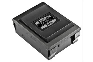
This programmable rocker switch includes a display that allows the system to dynamically change the context of the switch.

So, while using resistive and capacitive touch sensors are among the most common ways to implement a touch interface in consumer devices, they are not the only way. For example, NKK Switches offers programmable switches that integrate a push button or rocker switch with an LCD or OLED display. In addition to displaying icons and still images, some of these buttons can display a video stream. This allows the system to dynamically change the context of the button and communicate the context state to the user in an intuitive fashion. I am in the process of setting up some time with these programmable switches for a future write-up.

Another example of alternative sensing for touch interfaces is infrared sensors. The infrared proximity sensing offered by Silicon Labs and the infrared multi-touch sensing offered by Microsoft demonstrate the wide range of capabilities that infrared sensors can support at different price points.

Silicon Labs offers several kits that include infrared support. The FRONTPANEL2EK is a demo board that shows how to use capacitive and infrared proximity sensing in an application. The IRSLIDEREK is a demo board that shows how to use multiple infrared sensors together to detect not only the user’s presence, but also location and specific motion of the user’s hand. These kits are fairly simple and straightforward demonstrations. The Si1120EK is an evaluation platform that allows a developer to explore infrared sensing in more depth including advanced 3-axis touchless object proximity and motion sensing.

By working with these kits, I have a greater appreciation of the possible uses for proximity sensing. For example, an end device could place itself into a deep sleep or low power mode to minimize energy consumption. However, placing a system in the lowest power modes incurs a startup delay when reactivating the system. A smart proximity sensing system could provide the system with a few seconds warning that a user might want to turn the system on, and it could speculatively activate the device and be able to respond to the user more quickly. In this scenario, the proximity sensor would probably include some method to distinguish between likely power-up requests versus an environment where objects or people pass near the device without any intent of powering up the device.

Finally, Microsoft’s Surface product demonstrates the other end of touch sensing using an infrared camera system. In essence, the Surface is a true embedded vision system – an implementation detail that the end user does not need to know anything about. In the case of the Surface table, there are several infrared cameras viewing a diffusion surface. The diffusion surface has specific optical properties that allow the system software to identify when any object touches the surface of the display. This high end approach provides a mechanism for the end user to interact with the system using real world objects found in the environment rather than just special implements such as stylus with specific electrical characteristics.

The point here is to recognize that there are many ways to implement touch interfaces – including sonic mechanisms. They may not support touch interfaces in the same way, nor be able to support a minimum set of commands sets, but taken together, they may enable smarter devices that are able to better predict what the end user’s true expectations are and prepare accordingly. What other examples of alternative touch sensing technologies are you aware of?