What makes an embedded design low power?

Wednesday, March 2nd, 2011 by Robert Cravotta

It seems that nearly everything these days is marketed as a low power device/system. I see it so much in marketing material and in so many unsubstantiated contexts that it has become one of those phrases words that becomes invisible on the page or screen that I am reading. It is one of those terms that lack a set-in-concrete context – rather, it is often used as an indication of the intent of a device’s designers. Is it reasonable to declare an mW device as low power when there are μW devices in existence? Is it ever reasonable to declare a multi-watt system as low power?

The fact that low power thresholds are moving targets makes it more difficult to declare a system as low power – meaning that what is considered low power today soon becomes normal and the threshold of what constitutes low power necessarily shifts.

I recently was asked to build an online course about low power design for a processor that consumes power on the order of Watts. When I think of low power designs, I usually think of power consumption that is several orders of magnitude lower than that. While low power is not defined as a specific threshold, it can be addressed with appropriate techniques and strategies based on the context of the end design. I came up with an energy consumption spectrum that consists of six major categories. Even though the specific priorities for low power are different for each category, the techniques to address those priorities are similar and combined in different mixes.

We will be rolling out a new approach (that will eventually become fully integrated within the Embedded Processing Directory) for describing and highlighting low power features incorporated within microprocessors (including microcontrollers and DSPs) to enable developers to more easily identify those processors that will enable them to maximize the impact of the type of low power design they need.

What do you think is necessary to consider an embedded design as low power? Are there major contexts for grouping techniques and strategies for a set of application spaces? For example, energy harvesting applications are different from battery powered devices, which are different again from devices that are plugged into a wall socket. In some cases, a design may need to complete a function within a maximum amount of energy while another may need to limit the amount of heat is generated from performing a function. What are the different ways to consider a design as a low power one?

Will Watson affect embedded systems?

Wednesday, February 23rd, 2011 by Robert Cravotta

IBM’s Watson computer system recently beat two of the strongest Jeopardy players in the world in a real match of Jeopardy. The match was the culmination of four years of work by IBM researchers. This week’s question has a dual purpose – to focus discussion on how the Watson innovations can/will/might affect the techniques and tools available to embedded developers – and to solicit questions from you that I can ask the IBM research team when I meet up with them (after the main media furor dies down a bit).

The Watson computing system is the latest example of innovations in extreme processing problem spaces. The NOVA’s video “Smartest Machine on Earth” provides a nice overview of the project and the challenges that the researchers faced while getting Watson ready to compete against human players in the game Jeopardy. While Watson is able to interpret the natural language wording of Jeopardy answers and tease out appropriate responses for the questions (Jeopardy provides answers and contestants provide the questions), it was not clear from the press material or the video that Watson was performing processing of natural language in audio form or only text form. A segment near the end of the NOVA video casts doubt on whether Watson was able to work with audio inputs.

In order to bump Watson’s performance into the champion “cloud” (a distribution presented in the video of the performance of Jeopardy champions), the team had to rely on machine learning techniques so that the computing system could improve how it recognizes the many different contexts that apply to words.Throughout the video, we see that the team kept adding more pattern recognition engines (rules?) to the Watson software so that it could handle different types of Jeopardy questions. A satisfying segment in the video was when Watson was able to change its weighting engine for a Jeopardy category that it did not understand after receiving the correct answers of four questions in that category – much like a human player would refine their understanding of a category during a match.

Watson uses 2800 processors, and I estimate that the power consumption is on the order of a megawatt or more. This is not a practical energy footprint for most embedded systems, but the technologies that make up this system might be available to distributed embedded systems if they can connect to the main system. Also, consider that the human brain is a blood-cooled 10 to 100 W system – this suggests that we may be able to drastically improve the energy efficiency of a system like Watson in the coming years.

Do you think this achievement is huff and puff? Do you think it will impact the design and capabilities of embedded systems? For what technical questions would you like to hear answers from the IBM research team in a future article?

Boosting energy efficiency – How microcontrollers need to evolve

Monday, February 21st, 2011 by Oyvind Janbu

Whatever the end product, all designers have specific tasks to solve and their solutions will be influenced by the resources that are available and the constraints of cost, time, physical size and technology choice.  At the heart of many a good product, the ubiquitous microcontroller often has a crucial influence on system power design and particularly in a brave new world that’s concerned with energy efficiency, users are entitled to demand a greater service from them.  The way microcontrollers are built and operate needs to evolve dramatically if it is to achieve the best possible performance from limited battery resources.

Bearing in mind that the cost of even a typical coin cell battery can be relatively high compared to that of a microcontroller, there are obvious advantages in designing a system that offers the best possible energy efficiency.  It can enable designers to reduce the cost and size of a battery.  Secondly, it can enable designers to significantly extend the lifetime of a battery, consequently reducing the frequency of battery replacement and for certain products the frequency, cost and ‘carbon footprint’ associated with product maintenance call-outs.

Microcontrollers, like many other breeds of electronic components, are these days very keen to stress their ‘ultra low power’ credentials, which is perfectly fine and appropriate where a device’s dynamic performance merits; however, with a finite amount of charge available from a battery cell, it is how a microcontroller uses energy (i.e. power over the full extent of time), that needs to be more closely borne in mind.

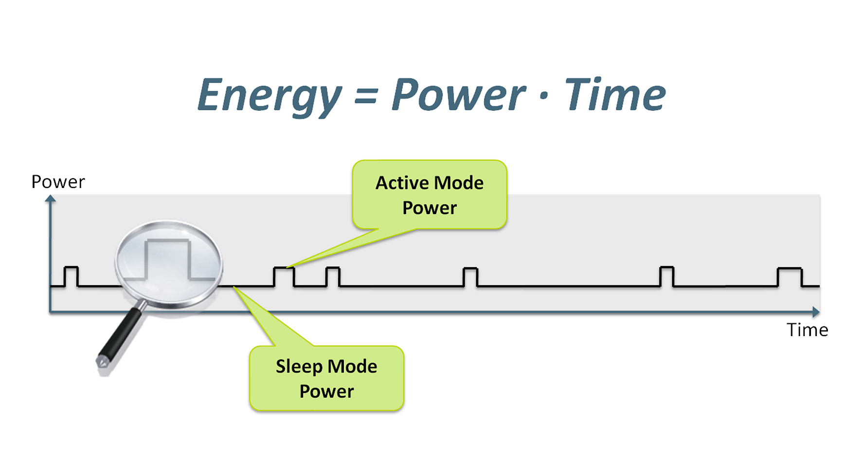
Microcontroller applications improve their energy efficiency by operating in several states – most notably active and sleep modes that consume different amounts of energy.

Product designers need to minimize the product of current and time over all phases of microcontroller operation, throughout both active and sleep periods (Figure 1). Not only does every microamp count, but so does every microsecond that every function takes.  This relationship between amperage and time makes the comparison of 8-, and 16-bit microcontrollers with 32-bit microcontrollers less straightforward. Considering alone their current consumption characteristics in a deep-sleep mode, it is easy to understand why 8-bit or 16-bit microcontrollers have been in an attractive position in energy sensitive applications, where microcontroller duty cycles can be very low.  A microcontroller may after all stay in a deep sleep state for perhaps 99% of the time.

However, if product designers are concerned with every microamp and microsecond every function takes, then using a 32-bit microcontroller should be being considered for even in the ‘simplest’ of product designs.  The higher performance of 32-bit processors enables the microcontroller to finish tasks quicker so that they can spend more time in the low-power sleep modes, which lowers overall energy consumption.  32-bit microcontrollers are therefore not necessarily ‘application overkill’.

More than that though, even simple operations on 8-bit or 16-bit variables can need the services of a 32-bit processor if system energy usage goals are to be achieved.  By harnessing the full array of low-power design techniques available today, 32-bit cores can offer a variety of low-power modes with rapid wake-up times that areon par with 8-bit microcontrollers.

There is a common misconception that switching from an 8-bit microcontroller to a 32-bit microcontroller will result in bigger code size, which directly affects the cost and power consumption of end products.  This is borne of the fact that many people have the impression that 8-bit microcontrollers use 8-bit instructions and 32-bit microcontrollers use 32-bit instructions.  In reality, many instructions in 8-bit microcontrollers are 16-bit or 24-bit in length.

The ARM Cortex-M3 and Cortex-M0 processors are based on the Thumb-2 technology, which provides excellent code density.  Thumb-2 microcontrollers have 16-bit as well as 32-bit instructions, with the 32-bit instruction functionality a superset of the 16-bit version.  Typical output from a C compiler gives 90% 16-bit instructions. The 32-bit version would only be used when the operation cannot be performed with a 16-bit instruction.  As a result, most of the instructions in an ARM Cortex microcontroller program are 16-bits.  That’s smaller than many of the instructions in 8-bit microcontrollers, typically providing less compiled code from a 32-bit processor than 8- or 16-bit microcontrollers.

The second part in this three part series looks deeper at the issues around microcontroller sleep modes.

Is embedded security necessary?

Wednesday, February 16th, 2011 by Robert Cravotta

I recently had an unpleasant experience related to online security issues. Somehow my account information for a large online game had been compromised. The speed in which the automated systems detected that the account had been hacked into and locked it down is a testament to how many compromised accounts this particular service provider handles on a daily basis. Likewise, the account status was restored with equally impressive turn-around time.

What impacted me the most about this experience was realizing that there is obviously at least one way that malicious entities can compromise a password protected system despite significant precautions to prevent such a thing from occurring. Keeping the account name and password secret; employing software to detect and protect against viruses, Trojan horses, or key loggers; as well as ensuring that data between my computer and the service provider is encrypted was not enough to keep the account safe.

The service provider’s efficiency and matter-of-fact approach to handling this situation suggests there are known ways to circumvent the security measures. The service provider offers and suggests using an additional layer of security by using single-use passwords from a device they sell for a few bucks and charge nothing for shipping.

As more embedded systems support online connectivity, the opportunity for someone to break into those systems increases. The motivations for breaking into these systems are myriad. Sometimes, such as in the case of my account that was hacked, there is the opportunity for financial gain. In other cases, there is notoriety for demonstrating that a system has vulnerability. In yet other cases, there may be the desire to cause physical harm, and it is this type of motivation that begs this week’s question.

When I first started working with computers in a professional manner, I found out there were ways to damage equipment through software. The most surprising example involved making a large line printer destroy itself by sending a particular sequence of characters to the printer such that it would cause all of the carriage hammers to repeatedly strike the ribbon at the same time. By spacing the sequence of characters with blank lines, a print job could actually make a printer that weighed several hundred pounds start rocking back and forth. If the printer was permitted to continue this behavior, mechanical parts could be severely damaged.

It is theoretically possible to perform analogous types of things with industrial equipment, and with more systems connected to remote or public networks, the opportunities for such mischief are real. Set top boxes that are attached to televisions are connecting to the network – offering a path for mischief if the designers of the set top box and/or television unintentionally left an opening in the system for someone to exploit.

Is considering the security implications in an embedded design needed? Where is the line between when implementing embedded security is important versus when it is a waste of resources? Are the criteria for when embedded security is needed based on the end device or on the system that such device operates within? Who should be responsible for making that call?

How to add color to electronic ink

Tuesday, February 15th, 2011 by Robert Cravotta

Over the past few years, electronic ink has been showing up in an increasing number of end-user products. Approximately ten years ago, there were a couple of competing approaches to implementing electronic ink, but E-Ink’s approach has found the most visible success of moving from the lab and viably existing in production level products, such as e-readers, indicators for USB sticks or batteries, as well as watch, smart card, and retail signage displays.

As a display technology, electronic ink exhibits characteristics that distinguish it from active display technologies. The most visible difference is that electronic ink exhibits the same optical characteristics as the printed page. Electronic ink displays do not require back or front lights; rather, they rely on reflecting ambient light with a minimum of 40% reflectivity. This optical quality contributes to a wider viewing angle (almost 180 degrees), better readability over a larger range of lighting conditions (including direct sunlight), and lower energy consumption because the only energy consumed by the display is to change the state of each pixel. Once an image is built on a display, it will remain there until there is another electrical field applied to the display – no energy is consumed to maintain the image. The switching voltage is designed around +/- 15 V.

However, electronic ink is not ideal for every type of display. The 1 to 10 Hz refresh rate is too slow for video. Until recently, electronic ink displays only supported up to 16 levels of grey scale monochrome text and images. The newest electronic ink displays now support up to 4096 colors (with 4-bit CR bias) along with the 16 levels of grey scale. Interestingly, adding support for color does not fundamentally change the approached used to display monochrome images.

The pigments and the chemistry are exactly the same between monochrome and color display; however, the display structure itself is different. The display is thinner so that it can be closer to a touch sensor to minimize parallax error that can occur based on the thickness of the glass over the display (such as with an LCD). Additionally, the display adds a color filter layer on the display and refines the process for manipulating the particles within each microcapsule.

The positively charged white particles reflect light while the negatively charged black particles absorb light.

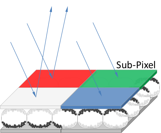
The 1.2 mm thick electronic ink display consists of a pixel electrode layer, a layer of microcapsules, and a color filter array (Figure 1). The electrode layer enables the system to attract and repel the charged particles within each of the microcapsules to a resolution that exceeds 200 DPI (dots per inch). Within each microcapsule are positively charged white particles and negatively charged black particles which are all suspended within a clear viscous fluid. When the electrode layer applies a positive or negative electric field near each microcapsule, the charged particles within it move to the front or back of the microcapsule depending on whether it is attracted or repelled from the electrode layer.

When the white particles are at the top of the microcapsule, the ambient light is reflected from the surface of the display. Likewise, when the black particles are at the top of the microcapsule, the ambient light is absorbed. Note that the electrode does not need to align with each microcapsule because the electric field affects the particles within the microcapsule irrespective of the border of the capsule; this means that a microcapsule can have white and black particles at the top of the capsule at the same time (Figure 2). By placing a color filter array over the field of microcapsules, it becomes possible to select which colors are visible by moving the white particles under the appropriate color segments in the filter array. Unlike the microcapsule layer, the electrode layer does need to tightly correlate with the color filter array.

The color filter array consists of a red, green, blue, and white sub-pixel segment at each pixel location. Controlling the absorption or reflection of light at each segment yields 4096 different color combinations.

This display uses an RGBW (Red, Green, Blue, and White) color system that delivers a minimum contrast ratio of 10:1 (Figure 2). For example, to show red, you would bring the white particles forward in the microcapsules under the red segment of the filter array while bringing the black particles forward in the other segments of the array. To present a brighter red color, you can also bring the white particles forward under the white segment of the filter array – however, the color will appear less saturated. To present a black image, the black particles are brought forward under all of the color segments. To present a white image, the white particles are brought forward under all of the color segments because under the RGBW color system, white is the result of all of the colors mixed together.

As electronic ink technology continues to mature and find a home in more applications, I expect that we will see developers take advantage of the fact that these types of displays can be formed into any shape and can be bent without damaging them. The fact that the color displays rely on the same chemistry as the monochrome ones suggests that adding color to a monochrome-based application should not represent a huge barrier to implement. However, the big challenge limiting where electronic ink displays can be used is how to implement the electrode layer such that it still delivers good enough resolution in whatever the final shape or shapes the display must support.

Can we reliably predict the winners?

Wednesday, February 9th, 2011 by Robert Cravotta

The Super Bowl played out this weekend and the results were quite predictable – one team won and the other lost. What was less predictable was knowing which of those teams would end up in the win column. Depending on their own set of preferences, insights, and luck, many people “knew” which team would win before the game started, but as the game started and continued toward the final play of the game, many people adjusted their prediction – even against their own wishes – as to the eventual outcome of the game.

Now that this shared experience is passed, I think it appropriate to contemplate how well we can, as individuals and as an industry, reliably predict the success of projects and technologies that we hope for and rely on when designing embedded systems. I think the exercise offers additional value in light of the escalating calls for public organizations to invest more money to accelerate the growth of the right future technologies to move the economy forward. Can we reliably predict which technologies are the correct ones to pour money into (realizing that we would also be choosing which technologies to not put research money into)? In effect, can and should we be choosing the technology winners and losers before they have proven themselves in the market?

Why does it seem that a company, product, or technology gets so much hype just before it falls? Take for example Forbes Company of the Year recipients Monsanto and Pfizer which appeared to be on top of the world when the award was given to them and then almost immediately afterwards faced a cascade of things going horribly wrong. I will only point out that competition in the smartphone market and tablet computing devices has gotten much more interesting in the past few months.

I remember seeing a very interesting television documentary on infomercials called something like “deal or no deal”. I would like to provide a link to it, but I cannot find it, so if you know what I am referring to please share. The big take away for me was one segment where a 30 year veteran in the infomercial world is asked if he knows how to pick the winners. The veteran replied that the success rate in the market is about 10% – meaning that of the products he down selects to and actually brings to market, only 10% are successful. Despite his insights into how the market responds to products, he could not reliably identify which products would be the successful ones – luck and timing still played a huge role in a product’s success.

Luck and timing are critical. Consider that the 1993 Simon predates the iPhone by 14 years and included similar features that made the iPhone stand out when it was launched including a touch screen.Mercata predates Groupon, which Google recently acquired for $2.5 billion, by almost a decade; timing differences with other structures in the market appear to have played a large role in the difference between the two company’s successes. In an almost comical tragedy, the precursor to the steam engine that was perfected by Hero (or Heron) of Alexandria and used in many temples in the ancient world, barely missed the perfect applications at Diolkos – and we had to wait another 1500 years for the steam engine to be reinvented and applied to practical rather than mystical applications.

I meet many people on both sides of the question, should we publicly fund future technologies to accelerate their adoption. My concern is that the track record of anyone reliably predicting the winners is so poor that we may be doing no better than chance – and possibly worse – when we have third party entities direct money that is not their own to projects they think may or should succeed. What do you think – can anyone reliably pick winners well enough to be trusted to do better than chance and allocate huge sums of money to arbitrary winners that still need to stand up to the test of time? What are your favorite stories of snatching failure from the jaws of victory?

Forward to the Past: A Different Way to Cope with Dark Silicon

Tuesday, February 8th, 2011 by Max Baron

Leigh’s comment to whether dark silicon is a design problem or fundamental law presents an opportunity to explore an “old” processor architecture, the Ambric architecture, an architecture whose implementation made use of dark silicon but did not escape the limitations imposed on Moore’s Law by power budgets.

Mike Butts introduced the Ambric architecture at the 2006 Fall Microprocessor Forum, an event at which I served as technical content chairperson. Tom Halfhill, my colleague at the time, wrote an article about Ambric’s approach and in February 2007 Ambric won In-Stat’s 2006 Microprocessor Report Analysts’ Choice Award for Innovation.

I’ll try to describe the architecture for those that are not familiar with it.

The Ambric’s architecture’s configuration went beyond the classical MIMD definition. It was described as a globally asynchronous – locally synchronous (GALS) architecture — a description that for chip designers held connotations of clock-less processing. The description however does not detract in any way from the innovation and the award for which I voted.

The streaming Ambric architecture as I saw it at the time could be described as a heterogeneous mix of two types of processing cores plus memories and interconnect.

Ambric’s programming innovation involved software objects assigned to specific combinations of cores and/or memory whose execution could proceed in their own time and at their own clock rate– this probably being the reason for the software-defined term “asynchronous architecture.” But the cores were clocked and some could be clocked at different rates—but probably in sync to avoid metastability.

The two types of processor cores provided by Am2045 — the chip introduced at the event — were described as SRs (Streaming RISC) engaged mainly in managing communications and utilities for the second type of cores, the high performance SRDs (Streaming RISC with DSP Extensions) that were the heavy lifter cores in the architecture.

Perhaps the most important part of Ambric’s innovation was the concept of objects assigned to combinations of one or more cores that could be considered as software/hardware black boxes. The black boxes could be interconnected via registers and control that made them behave as if they were FIFOs.

I believe that this is the most important part of the innovation because it almost removes the overhead of thread synchronization. With the removal of this major obstacle to taking advantage of highly parallelizable workloads such as encountered in DSP applications, Ambric opened the architecture for execution by hundreds and possibly thousands of cores — but at the price of reduced generality and the need of more human involvement in the routing of objects on interconnects for best performance of processor cores and memory.

The Ambric architecture can cover with cores and memories a die that for example provides at a lower technology node, four times more transistors but the architecture can’t quadruple its computing speed (switchings per second) due to power budget limitations be they imposed by temperature limitations or battery capacity. Designers can only decrease the chip’s VDD to match a chip’s power dissipation to its power budget, but in doing so, they must reduce clock frequency and associated performance.

The idea of connecting “black boxes” originated with designers of analog computers and hybrid analog/digital computers at least 60 years ago. It was the approach employed in designing computers just before the introduction of the Van Neumann architecture. Ambric’s innovation that created a software/hardware combination is probably independent of the past.

Compared with Ambric’s approach, the UCSD/MIT idea is based on a number of compiler-created different efficient small cores specialized to execute short code sequences critical to the performance of the computer. The UCSD/MIT architecture can enjoy more generality in executing workloads on condition that some specific small cores must be created for the type of workloads targeted. By raising small core frequency without creating dangerous hot spots, the architecture can deliver performance yet keep within power budget boundaries – but it too, can’t deliver increased compute performance at the same rate as Moore’s law delivers transistors.

Is assembly language a dead skillset?

Wednesday, February 2nd, 2011 by Robert Cravotta

Compiler technology has improved over the years. So much so that the “wisdom on the street” is that using a compiled language, such as C, is the norm for the overwhelming majority of embedded code that is placed into production systems these days. I have little doubt that most of this sentiment is true, but I suspect the “last mile” challenge for compilers is far from being solved – which prevents compiled languages from completely removing the need for developers that are expert at assembly language programming.

In this case, I think the largest last mile candidate for compilers is managing and allocating memory outside of the processor’s register space. This is a critical distinction because most processors, except the very small and slower ones, do not provide a flat memory space where every memory access possible takes a single clock cycle to complete. The register file, level 1 cache, and tightly coupled memories represent the fastest memory on most processors – and those memories represent the smallest portion of the memory subsystem. The majority of a system’s memory is implemented in slower and less expensive circuits – which when used indiscriminately, can introduce latency and delays when executing program code.

The largest reason for using cache in a system is to hide as much of the latency in the memory accesses as possible so as to be able to keep the processor core from stalling. If there was no time cost for accessing anywhere in memory, there would be no need to use a cache.

I have not seen any standard mechanism in compiled languages to layout and allocate an application’s storage elements into a memory hierarchy. One problem is that such a mechanism would make the code less portable – but maybe we are reaching a point in compiler technology where that type of portability should be segmented away from code portability. Program code could consist of a portable code portion and a target-specific portion that enables a developer to tell a compiler and linker how to organize the entire memory subsystem.

A possible result of this type of separation is the appearance of many more tools that actually help developers focus on the memory architecture and find the optimum way to organize it for a specific application. Additional tools might arise that would enable developers to develop application-specific policies for managing the memory subsystem in the presence of other applications.

The production alternate at this time seems to be systems that either accept the consequences of sub-optimally automated memory allocation or to impose policies that prevent loading applications onto the system that have not been run through a certification process that makes sure each program behaves to some set of memory usage rules. Think of running Flash programs on the iPhone (I think the issue of Flash on these devices is driven more by memory issues – which affect system reliability – than by dislike of another company).

Assembly language programming seems to continue to reign supreme for time sensitive portions of code that rely on using a processor’s specialized circuits in an esoteric fashion and/or rely on an intimate knowledge of how to organize the storage of data within the target’s memory architecture to extract the optimum performance from the system from a time and/or energy perspective. Is this an accurate assessment? Is assembly language programming a dying skillset? Are you still using assembly language programming in your production systems? If so, in what capacity?

Dark Silicon Redux: System Design Problem or Fundamental Law?

Tuesday, February 1st, 2011 by Max Baron

Like a spotlight picking out an object in total darkness, the presentation of a solution to a problem may sometimes highlight one aspect while obscuring others. Such were the dark silicon problem and the solution by UCSD and MIT that was presented at Hot Chips 2010. Such was also the article I published in August describing the two universities’ idea that could increase a processor’s efficiency.

At the time of that writing, it appeared that the idea would be followed in time by many others that together would overcome the dark silicon problem. All would be well: Moore’s Law that provides more transistors would also provide higher compute performance.

The term ‘dark silicon’ was probably coined by ARM. ARM described dark silicon as a problem that must be solved by innovative design, but can it be completely solved?Can design continue to solve the problem ‘forever’? To answer the question, we next try to take a qualitative look at the dependencies among the system, the die, and compute performance.

According to a 2009 article published in EE Times, ARM CTO Mike Muller said: “Without fresh innovations, designers could find themselves by 2020 in an era of ‘dark silicon,’ able to build dense devices they cannot afford to power.” Mr. Muller also noted in the same article that“ . . . a 11nm process technology could deliver devices with 16 times more transistors . . . but those devices will only use a third as much energy as today’s parts, leaving engineers with a power budget so pinched they may be able to activate only nine percent of those transistors.”

The use of “only” in the quote may be misunderstood to indicate lower power consumption and higher efficiency. I believe that it indicated disappointment that compared with today’s parts the power consumption would not drop to at least one sixteenth of its 2009 value — to match the rise in the number of transistors.

The term “power budget” can have more than one interpretation. In tethered systems pursuing peak-performance, it can be the worst-case power that is die-temperature related. In mobile systems, it may have a different interpretation: it may be related to the battery-capacity and the percentage of overall system power allocated to the processor. Both interpretations will limit a chip’s power-performance but the limiting factors will be different.

The architects at UCSD/MIT made the best of the unusable silicon problem by surrounding a general-purpose processor core with very efficient small cores located in the dark silicon area. The cores could execute very short sequences of the application code faster and more efficiently than a general-purpose processor but, to keep within the boundary of a power budget, they were probably activated only when needed by the program.

The universities have shown a capability to use part of the dark silicon transistors. It would be interesting to find whether, as transistor numbers increase, the power budget might be dictated by some simple parameters. Finding some limits would rule out dark silicon as a mere problem whose solution will allow designers to utilize 100% of a die to obtain increased performance. In some implementations, the limits could define the best die size and technology of a SoC.

In a system willing to sacrifice power consumption for performance the power budget should be equal to or smaller than the power that can be delivered to the die without causing damage. It is the power (energy/time) that in steady state can be removed from the die by natural and forced cooling, without raising the die’s temperature to a level that would reduce the die’s reliability or even destroy it.

If we allow ourselves the freedom sometimes employed by physicists in simplifying problems, we can say that for a uniformly cooled die of infinite heat conductivity (hot spots can’t occur), the heat generated by circuits and therefore the power budget, are both distributed evenly across the area of the die and are proportional to it (Pbudget α Adie  . . . the larger the die the higher the power budget).

Simplifying things once more, we define a die-wide average energy Eavg in joules required for one single imaginary circuit (the average circuit) to switch state. The power budget (energy divided by time) can now be expressed as the power consumed by the single circuit: Pbudget ~ f * Eavgwhere f is the frequency of switching the single average circuit. The actual frequency of all logic on the chip would be factual = f / n where n is the average number of switchings occurring at the same time.

In other words, assumingdie-area cooling, with all other semiconductor conditions (a given technology node, fabrication, leakage, environment parameters and the best circuit design innovations) and cooling – all kept constant — the peak computing performance obtainable (allowable number of average switching per second) is directly related to the die area. Else the chip will be destroyed.The fate of 3D multi-layer silicon will be worse since the sandwiched layers will enjoy less cooling than the external layers.

Power budgets assigned to processors in mobile systems are more flexible but can be more complex to determine. Camera system designers, for example, can trade-off finder screen size and brightness or fps (frames per second), or zoom and auto focus during video capture — for more processor power. Smart phones that allow non-real-time applications to run slower can save processor power. And, most mobile systems will profit from heterogeneous configurations employing CPUs and hard-wired low power accelerators.

Power budgets in mobile systems will also be affected by software and marketing considerations. Compilers affect the energy consumed by an application based on the number and kind of instructions required for the job to complete. Operating systems are important in managing a system’s resources and controlling the system power states. And, in addition to software and workload considerations the ‘bare core’ power consumption associated with a SoC must compete with claims made by competitors.

If local die temperature and power dissipation terminated the period where higher clock frequency meant more performance, the limitations imposed by allocated power budget or die area will curtail the reign of multiple core configurations as a means of increasing performance.

Most powerful 3D computer

Many computer architects like to learn from existing architectures. It was interesting therefore to see how the most powerful known 3D computer is working around its power limitations. It was however very difficult to find much data on the Internet. The data below was compiled from a few sources and the reader is asked to help corroborate it and/or provide more reliable numbers and sources:

An adult human brain is estimated to contain 1011 (100 Billion) neurons. A firing neuron consumes an average energy of 10-9 joules.  The neuron’s maximum firing rate is estimated by some papers to be 1,000Hz. Normal operating frequencies are lower at 300Hz to 400Hz.

The maximum power that would be generated by the human brain with all neurons firing at the maximum frequency of 1,000 Hz is 103 * 1011* 10-9 = 105 joule/second = 100,000 Watt — enough to destroy the brain and some of its surroundings.

Some papers estimate the actual power consumption of the brain at 10W while others peg it at 100W. According to still other papers the power averaged over 24 hours is 20W. Yet, even the highest number seems acceptable since the brain’s 3D structure is blood-and-evaporation cooled and kept at optimal temperature. Imagine keeping a 100W heat source cool by blood flow!  Performance-wise the 10W and 100W power estimates imply that the brain is delivering 1010 or 1011 neuron firings per second. Using the considerations applied to semiconductor die usage, the brain may be running at 0.01% or up to 0.1% of its neuron capacity possibly turning semi-“dark brain” sections fully “on” or partly “off” depending on workload. Compare these percentages with the much higher 9% utilization factor forecasted for 11nm silicon.

The highly dense silicon chip and the human brain are affected by the same laws of physics.

In semiconductor technology, as Moore’s law places more transistors on the same-sized die or makes the die smaller, the power budget needed for full transistor utilization moves in the opposite direction since it requires larger die areas.Unless cost-acceptable extreme cooling can track technology nodes by removing for example at 11nm about five times more heat from the reference die, or technology finds ways to reduce a cores’ power dissipation by the same factor, Moore’s Law and computing performance will be following different roadmaps.

In mobile applications the limit is affected by battery capacity vs. size and weight. According to some battery developers, capacity is improving slowly as vendors spend more effort in creating custom batteries for big suppliers of mobile systems — than in research. I’m estimating battery capacity to improve at approximately 6% per year, leaving Moore’s law without support since it doubles transistor numbers every two years.

UCSD/MIT’s approach is not a ‘waste’ of transistors if its use of dark silicon can deliver higher performance within the boundaries of the power budget.The Von Neumann architecture was built to save components since it was created at a time when components were expensive, bulky and hard to manufacture. Our problem today and in the near future is to conceive of an architecture that can use an affluence of components.

Debugging Stories: Development Tools

Monday, January 31st, 2011 by Robert Cravotta

Anyone that has developed a system has debugging stories. A number of those stories are captured in the responses to a Question-of-the-Week posed a while ago about your favorite debugging anecdote. While collecting the different stories together reveals some worthwhile lessons learned, reading through all of the stories can be time consuming and random as to the type of content in each story. This article, and future others like it, will attempt to consolidate a class of debugging stories together to ease access for you. The rest of this article will focus on the stories and lessons based around issues with the development tools.

In reading through the stories, I am reminded that I worked with a C cross compiler that did not generate the proper code for declaring and initializing float variables. The work around was to avoid initializing the float variable as part of the declaration. The initialization had to be performed as a distinct and separate assignment within the body code. Eventually, within a year of us finding the problem, the company that made the compiler fixed it, but I continued to maintain the code so as to keep the declaration and initialization separate. It felt safer to the whole development team to comment the initialization value with the declaration line and place all of the initialization code at the beginning of the code block.

Two stories identified how the debugger can misrepresent how the actual runtime code executes with and without the debugger in the system. Andrew Coombes shared a story about how the debugger inappropriately assumed when a block of code had the same CRC value as the previously loaded code that it was identical and skipped the process of loading the new code onto the target. The problem was exacerbated by the fact that the debugger did not calculate the CRC correctly. S.B. @ LI shared a story where the debugger was intercepting and correcting the data types in a call structure to an operating system call. This masked the real behavior of the system when the debugger was not active where the data types were not correct.

There were stories about compilers that would allocate data to inappropriate or unavailable memory resources. RSK @ LI shared how he had to use an inline-like function using preprocessor macros to reduce the call depth to avoid overflowing the hardware stack. E.P. @ LI’s story does not specify whether the compiler set the cache size, but the debugged code used a cache block that was one database block large and this inappropriate sizing caused the database application to run excessively slow. R.D @ LI recounts how a compiler was automatically selecting a 14-bit register to store a 16-bit address value, and how adding a NOP in front of the assignment cause the compiler to choose the correct register type to store the value.

I recall hearing many admonishments when I was a junior member of the staff to not turn on the compiler optimizations. I would hear stories about compiler optimizations that did not mix well with processor pipelines that did not include interlocks, and the horrible behaviors that would ensue. J.N. @ LI recounts an experience with a compiler optimization that scheduled some register writes just before a compare so that the system behaved incorrectly.

M.B. @ LI reminds us that even library code that has been used for long periods of time over many projects can include latent problems – especially for functions embedded within libraries, such as newlib in this case. L.W. @ LI’s story tells of when he found a NULL pointer access that had been within a seldom activated conditional with a library call.

I like J.N. @ LI‘s summary – “Different tools have different strengths, which is why you learn to use several and switch off when one isn’t finding the problem. And sometimes one tool gives you a hint that gets you closer, but it takes a different tool (or tools) to get you the rest of the way.”

Please let me know if you find this type of article useful. If so, I will try to do more on the topics that receive large numbers of responses that can be grouped into a smaller set of categories.