Articles by Robert Cravotta

As a former Technical Editor covering Embedded Processing at EDN, Robert has been following and commenting on the embedded processing space since 2001 (see article index). His expertise includes software development and system design using microprocessors, microcontrollers, digital signal processors (DSPs), multiprocessor architectures, processor fabrics, coprocessors, and accelerators, plus embedded cores in FPGAs, SOCs, and ASICs. Robert's embedded engineering background includes 16 years as a Member of the Technical Staff at Boeing and Rockwell International working on path-finding avionics, power and laser control systems, autonomous vehicles, and vision sensing systems.

Is peer code inspection worthwhile?

Wednesday, April 6th, 2011 by Robert Cravotta

I am a strong believer in applying multiple sets of eyes to tasks and projects. Design reviews provide a multi-stage mechanism for bringing independent eyes into a design to improve the probability of uncovering poor assumptions or missed details. Peer performed code inspection is another mechanism to bring multiple sets of eyes to the task of implementing software code. However, given the evolution of automated code checking tools, is the manual task of inspecting a peer’s code still a worthwhile task?

Even when tools were not readily available to check a developer’s code, my personal experience involved some worthwhile and some useless code inspection efforts. In particular, the time I engaged in a useless code inspection was not so much about the code, but rather about how the team leader approach the code inspection and micromanaged the process. That specific effort left a bad taste in my mouth for overly formal and generic procedures for a task that requires specific and deep knowledge to perform well.

A staggering challenge facing code inspectors is the sheer magnitude of software that is available for inspecting. The labor for inspecting software is significant and it requires a high level of special skills and knowledge to perform. Tools that perform automated code inspections have proliferated, and they continue to improve over time, but are they good enough alternative to peer code inspections? I like Jack Ganssle’s “Guide to Code Inspections”, but even his final statement in the article (“Oddly, many of us believe this open-source mantra with religious fervor but reject it in our own work.”) suggests that the actions of software developers imply that they do not necessarily consider code inspections a worthwhile redirection of development team’s time.

Is peer-based code inspection worthwhile? Are the automated code inspection tools good enough to replace peer inspection? When is peer inspection necessary, or in what ways is automated inspection insufficient?

When is single better than multiple?

Wednesday, March 30th, 2011 by Robert Cravotta

For decades, many embedded designs used separate processors for handling the signal and control processing. Part of the reason for using separate and different types of processors is that the data and processing characteristics of control and signal processing are different enough to warrant different implementations. Control processing is characterized by frequent context switches as the control software must handle different asynchronous events so as to minimize the latency between when an event occurs and when the controller responds to that event. Microcontroller architectures that specialize in control processing usually include circuitry that enables them to detect and respond to interrupts quickly and deterministically.

In contrast, signal processing is characterized by very few context switches. Rather, signal processing exhibits relatively repetitive and predictable processing – however, the amount of computing that must be performed at each data point is usually substantial and overloads traditional microcontroller architectures. Signal processing architectures trade-off efficient context switching for efficient loop processing via special loop instructions and data handling via additional buses.

Because controllers and signal processors differ so much at the architectural level, the skills required to program them are different and the tools to develop with them are different. Managing two different processors simplifies partitioning the processing tasks, but it also increases the complexity of integrating between the two processing systems for the design team.

Within the last decade, a hybrid processing architecture emerged that combined control and signal processing into a single instruction stream. The most recently used label for such processors is digital signal controllers (DSC) which acknowledges its combined architectural trade-offs. DSCs are able to perform context switching like a microcontroller, but they are also able to process light weight signal processing tasks better than a microcontroller. However, they are not capable of handling heavy-lifting signal processing as well as dedicated signal processing architectures.

Hybrid architectures and the development tools to work with them have matured. Hybrid architectures allow a development team to use the same processor architecture throughout each part of the design which supports using the same instruction set and same development tools. However, the interface between the controller and signal processing tasks is limited to the architectural trade-offs that the processor architect made. If the trade-offs that were made match the needs for the project it is being used in, then all is well, but any mismatch will affect the development team’s implementation options.

When is using the single instruction stream benefit of a DSC or hybrid architecture better than using the multiple instruction stream approach of multiple and different types of processors in a design? Have you made this trade-off decision with any of your designs? When did you choose one over the other and why?

Touch with the Microsoft Surface 2.0

Tuesday, March 29th, 2011 by Robert Cravotta

The new Microsoft Surface 2.0 will become available to the public later this year. The technology has undergone significant changes from when the first version was introduced in 2007. The most obvious change is that the dimensions of the newer unitis much thinner, so much so, that the 4 inch thick display can be wall mounted – effectively enabling the display to act like a large-screen 1080p television with touch capability.Not only is the new display thinner, but the list price has nearly halved to $7600. While the current production versions of the Surface are impractical for embedded developers, the sensing technology is quite different from other touch technologies and may represent another approach to user touch interfaces that will compete with other forms of touch technology.

Namely, the touch sensing in the Surface is not really based on sensing touch directly – rather, it is based on using IR (infrared) sensors the visually sense what is happening around the touch surface. This enables the system to sense and be able to interact with nearly any real world object, not just conductive surfaces such as with capacitive touch sensing or physical pressure such as with resistive touch sensing. For example, there are sample applications of the Surface working with a real paint brush (without paint on it). The system is able to identify objects with identification markings, in the form of a pattern of small bumps, to track those objects and infer additional information about them that other touch sensing technologies currently cannot do.

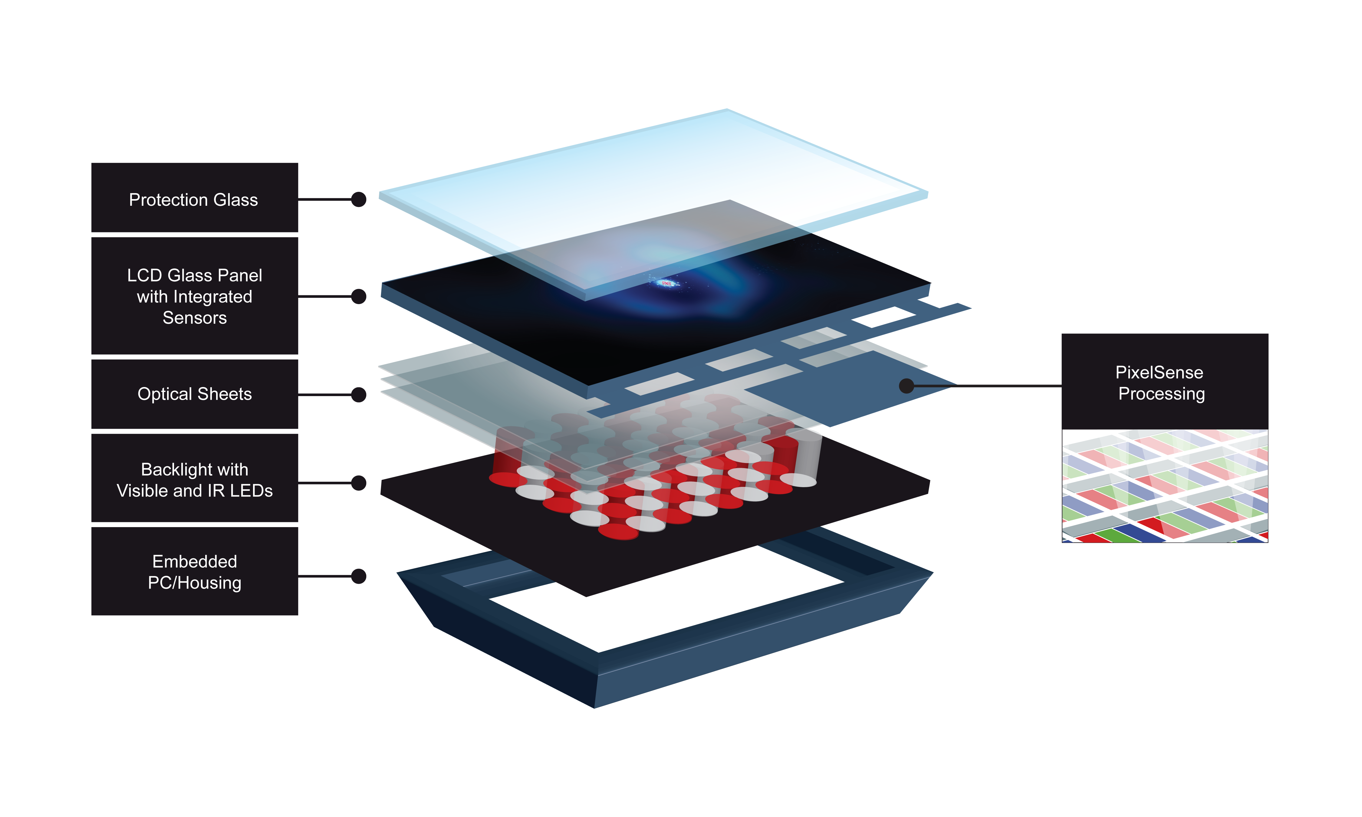
This exploded view of the Microsoft Surface illustrate the various layers that make up the display and sensing housing of the end units. The PixelSense technology is embedded into the LCD layers of the display.

The vision sensing technology is called PixelSense Technology, and it is able to sense the outlines of objects that are near the touch surface and distinguish when they are touching the surface. Note: I would include a link to the PixelSense Technology at Microsoft, but it is not available at this time. The PixelSense Technology embedded in the Samsung SUR40 for Microsoft Surface replaces the five (5) infrared cameras that the earlier version relies on. The SUR40 for Microsoft Surface is the result of a collaborative development effort between Samsung and Microsoft. Combining the Samsung SUR40 with Microsoft’s Surface Software enables the entire display to act as a single aggregate of pixel-based sensors that are tightly integrated with the display circuitry. This shift to an integrated sensor enables the finished casing to be substantially thinner than previous versions of the Surface.

The figure highlights the different layers that make up the display and sensing technology. The layers are analogous to any LCD display except that the PixelSense sensors are embedded in the LCD layer and do not affect the original display quality. The optical sheets include material characteristics to increase the viewing angle and to enhance the IR light transmissivity. PixelSense relies on the IR light generated at the backlight layer to detect reflections from objects above and on the protection layer. The sensors are located below the protection layer.

The Surface software targets an embedded AMD Athlon II X2 Dual-Core Processor operating at 2.9GHz and paired with an AMD Radeon HD 6700M Series GPU using DirectX 11 acting as the vision processor. Applications use an API (application program interface) to access the algorithms contained within the embedded vision processor. In the demonstration that I saw of the Surface, the system fed the IR sensing to a display where I could see my hand and objects above the protection layer. The difference between an object hovering over and touching the protection layer is quite obvious. The sensor and embedded vision software are able to detect and track more than 50 simultaneous touches. Supporting the large number of touches is necessary because the use case for the Surface is to have multiple people issuing gestures to the touch system at the same time.

This technology offers exciting capabilities for end-user applications, but it is currently not appropriate, nor available, for general embedded designs. However, as the technology continues to evolve, the price should continue to drop and the vision algorithms should mature so that they can operate more efficiently with less compute performance required of the vision processors (most likely due to specialized hardware accelerators for vision processing). The ability to be able to recognize and work with real world objects is a compelling capability that the current touch technologies lack and may never acquire. While the Microsoft person I spoke with says the company is not looking at bringing this technology to applications outside the fully integrated Surface package, I believe the technology will become more compelling for embedded applications sooner rather than later. At that point, experience with vision processing (different from image processing) will become a valuable skillset.

Low Power Design: Energy Harvesting

Friday, March 25th, 2011 by Robert Cravotta

In an online course about the Fundamentals of Low Power Design I proposed a spectrum of six categories of applications that identify the different design considerations for low power design for embedded developers. The spectrum of low power applications I propose are:

1) Energy harvesting

2) Disposable or limited use

3) Replaceable energy storage

4) Mobile

5) Tethered with passive cooling

6) Tethered with active cooling

This article focuses on the characteristics that affect energy harvesting applications. I will publish future articles that will focus on the characteristics of the other categories.

Energy harvesting designs represent the extreme low end of low power design spectrum. In an earlier article I identified some common forms of energy harvesting that are publicly available and the magnitude (typically in the μW to mW range) of the energy that are typically available for harvesting.

Energy harvesting designs are ideal for tasks that take place in locations that are difficult to deliver power. Examples include remote sensors, such as might reside in a manufacturing building where the quantity of devices might make performing regular battery replacements infeasible. Also, many of the sensors may be in locations that are difficult or dangerous for an operator to reach. For this reason, energy harvesting systems usually run autonomously, and they spend the majority of their time in a sleep state. Energy harvesting designs often trade-off computation capabilities to fit within a small energy budget because the source of energy is intermittent and/or not guaranteed on a demand basis.

Energy harvesting systems consist of a number of subsystems that work together to provide energy to the electronics of the system. The energy harvester is the subsystem that interfaces with the energy source and converts it into usable and storable electricity. Common types of energy harvesters are able to extract energy from ambient light, vibration, thermal differentials, as well as ambient RF energy.

The rate of energy captured from the environment by the energy harvester may not be sufficient to allow the system to operate; rather, the output of the energy harvester feeds into an energy storage and power management controller that conditions and stores the captured energy in an energy bladder, buffer, capacitor, or battery. Then, when the system is in an awake state, it is drawing energy from the storage module.

The asymmetry between the rate of collecting energy and consuming energy necessitates that the functions the system needs to perform are only executed on a periodic basis that allows enough new energy to be captured and stored between operating cycles. Microcontrollers that support low operating or active power consumption, as well as the capability to quickly switch between the on and off state are key considerations for energy harvesting applications.

A consideration that makes energy harvesting designs different from the other categories in the low power spectrum is that the harvested energy must undergo a transformation to be usable by the electronics. This is in contrast to systems that can recharge their energy storage – these systems receive electricity directly in quantities that support operating the system and recharging the energy storage module.

If the available electricity ever becomes insufficient to operate the energy harvesting module, the module may not be able to capture and transform ambient energy even when there is enough energy in the environment. This key condition for operating means the decision for when and how the system will turn on and off must take extra precautions to avoid drawing too much energy during operation or it will risk starving the system into an unrecoverable condition.

Energy harvesting applications are still an emerging application space. As the cost continues to decrease and the efficiency of the harvesting modules continues to improve, more applications will make sense to pursue in an analogous fashion that microcontrollers have been replacing mechanical controls within systems for the past few decades.

Which is better: faster- or quality-to-market?

Wednesday, March 23rd, 2011 by Robert Cravotta

There are at least two major schools of thought about the best way to release new products – especially products that contain software that can be updated by the user. The faster-to-market approach pushes designs through the development cycle as quickly as possible to release the new product to market before anyone else. A plausible tactic for faster-to-market products that have user-updatable software is to ship the product even while there are still major bugs in the system with the expectation that the development team can create a corrective software patch before the product actually ends up in the hands of the customer. In this scenario, the expectation is that the user will perform a software update before they can even use the product the first time.

The quality-to-market school of thought believes that products should work out of the box without requiring extra effort from the user such as downloading and applying software patches. This philosophy does not preclude the later use of software updates to add or improve features – rather, the out of the box experience is considered an important part of the product’s value.

An argument for the faster-to-market approach is that the user will be able to start benefiting from the product sooner – possibly months sooner because the development team is able to take advantage of the production lead time to bring the product to the desired level of performance. This argument often presumes that the development team would still be working on fixing bugs after shipping a finished product even under the quality-to-market approach. For this approach, the shorter term tactical advantage of using a capability sooner outweighs the probability that some expected features may not work properly.

Likewise, an argument for the quality-to-market approach is that the user will know for certain at the time of purchase what the product will and will not be able to perform. A presumption of this argument is that sometimes a faster-to-market product overpromises what the development team is able to deliver and this leads to customer dissatisfaction because of unmet expectations. For this approach, the longer term strategic advantage of always being able to use the features as-advertised outweighs the probability that a crippled version of the feature will cause you to lose future sales.

There are many companies that side with both of these schools of thought. Which is better? Is one always better or is there a condition when one approach is better than the other? How does your development cycle accommodate one or both of these approaches to releasing a product?

Do you have enough budget for your embedded project?

Wednesday, March 16th, 2011 by Robert Cravotta

The word on the street is that budgets for development projects have been shrinking for years – perhaps even decades. If this sentiment is true, how do so many embedded designs make it to production status each year? Is the design quality for these projects more compromised each year? If the projects are over budget each year, how do the companies that fund these projects realize a high enough return on investment to keep justifying starting new designs? I question the validity of the claim that budgets have been shrinking year-in and year-out for ever increasingly complex designs without some offset occurring somewhere.

Perhaps a development team has a smaller budget for developers, but is it done without an increase for the development tools? I have been watching the development tool industry for years to see where the big productivity gains are coming from. Most of what I have observed is incremental improvements in what tools can offload from developers. Also, I do believe companies have been slashing their training budgets, but somehow the projects still get done (maybe not optimally but well enough to justify doing the project in the first place).

Another way that projects might get by with smaller development budgets is through heavy reuse of earlier designs and/or licensed IP (intellectual property). A trend that I have seen increasing over the years is that semiconductor companies are providing more software with their silicon products so that development teams can concentrate their efforts on the value add features rather than the basic functions. In this case, the overall budget is not shrinking so much as it is being transferred to different development teams.

I do not expect that development teams have generous budgets. I do expect that the budgets routinely require creative thinking from the team members as to how to squeeze 10 to 20% more out of the budget to meet the project requirements – but that is the process by which continuous improvement occurs – I doubt it would occur any other way. Are your budgets sufficient or are they too tight to complete your projects? What would you change about your budgeting process if you had your way? Is it possible for budgets to shrink every year and still be able to produce ever more complex designs?

How do you handle obsolescence?

Wednesday, March 9th, 2011 by Robert Cravotta

Producers and users are both involved when a product, component, or technology is slated for obsolescence, but both parties do not always agree that the obsolescence is appropriate. Take for example Microsoft’s efforts to kill Internet Explorer 6 (IE6). The company recently launched a website called ie6countdown.com with the intent to track and encourage people to migrate away from the ten year old web browser. As of February 2011, 12% of worldwide users are still using IE6 as their browser – this represents a sizable group of people that present a support challenge for Microsoft and web content developers. According to Roger Capriotti at Microsoft, their goal is to get the worldwide share down to below 1% because they believe that 1% will allow more sites and IT pros worldwide to make IE6 a low-priority browser.

One thing I was not able to discover on the tracking website is the type of machine these IE6 users are running the browser on. I suspect that the underlying hardware may play a larger role in the continued use of the browser that will be three generations behind the latest browser (IE9) as of March 14th.

For embedded developers, the obsolescence of components can wreak havoc. While the end user may not even be aware of the embedded systems in their end devices, changing the implementation of an embedded system is no trivial task. That is why on many aerospace programs I worked on we specified that the microprocessor that we selected must be available to support a twenty or thirty year support window. Now that did not mean the processor supplier had to keep manufacturing those processors for all of those years, but it did mean that there was a plan to pre-produce and store those processors against some usage plan for that period of time.

Part of the reason for continuing to use the older processors was that it was too risky and expensive to upgrade the system to the latest generation processors. Even though a processor may be fully backwards compatible, the interfaces and timing differences of system events could shift just enough to cause intermittent failures in the end system. To upgrade a processor would entail a complete recertification, and for some systems, that is an unjustifiable expense to only maintain the functionality of a system.

Maintaining older generations of components beyond their production life cycle can also apply to software modules. Changing the operating system in an embedded system may also require a recertification, so it is safer and more cost effective to freeze the operating system at a specific configuration and version.

How do you handle obsolescence – both as a producer and as a user? As a producer, this question is most interesting when your user base wishes to continue using your product beyond your planned production cycle. As a user, this question is interesting as a way to explore different strategies to maintain a frozen design or migrate the design without incurring product killing costs.

Low Power Design Course

Tuesday, March 8th, 2011 by Robert Cravotta

In last week’s Question of the Week I asked “what makes an embedded design low power?” I asked if there was a way to describe low power design such that it accommodates moving the threshold definitions as technology continues to improve. The reader responses encompassed a common theme – that the magnitude of the system’s power consumption is not what defines it as a low power design. Rather, you must take into account the end-use requirements and compare the final implementation with other implementations for analogous functions to confirm that the “low power” implementation completes the function at less cost and/or less energy.

The impetus for this question comes from a new information center about the basics of design that we have added to Embedded Insights to supplement an online course that I recently put together and presented. The course is hosted at EE Times as part of their Fundamentals feature, and it is called Fundamentals of Low Power Design using the Intel Atom Processor.

A challenge in creating the course was to create an approach that imparted useful information to every type of embedded developer – not just the people that were interested in the target processor (the Intel Atom in this case). I developed a spectrum of low power design that expands the sweet spot concept that I have proposed for processor architectures. In this case, the spectrum identifies six (6) different target implementations that share a common goal and available techniques for low power/energy designs – but they may define their thresholds and optimization approaches differently. The categories identified in the spectrum are energy harvesting, disposable, replaceable, mobile, tethered with passive cooling, and tethered with active cooling. I briefly describe each of these categories in the course, and I will follow-up with articles that focus on each one.

The Basics Information Center aggregates and organizes information on the basics for design topics. The inaugural page includes a set of low power optimization datasheets for a number of processor architectures that I researched when developing the course – however, including them in the final version of the course material would disrupt the flow of the sponsored material, so we are providing them as supplemental material. The concepts in the datasheets are a work-in-progress, so we welcome any comments that help us to tweak and fill-in the content so that the lower power spectrum and datasheets become a more useful tool for describing embedded processors. The end goal is to take what we learn from this effort and incorporate it into a parts search engine for the Embedded Processing Directory.

The datasheets currently reflect the organization of the course material; we will probably need to change them to make the information more generally accessible. Please share any ideas or specific information that we can use to refine the datasheets.

What makes an embedded design low power?

Wednesday, March 2nd, 2011 by Robert Cravotta

It seems that nearly everything these days is marketed as a low power device/system. I see it so much in marketing material and in so many unsubstantiated contexts that it has become one of those phrases words that becomes invisible on the page or screen that I am reading. It is one of those terms that lack a set-in-concrete context – rather, it is often used as an indication of the intent of a device’s designers. Is it reasonable to declare an mW device as low power when there are μW devices in existence? Is it ever reasonable to declare a multi-watt system as low power?

The fact that low power thresholds are moving targets makes it more difficult to declare a system as low power – meaning that what is considered low power today soon becomes normal and the threshold of what constitutes low power necessarily shifts.

I recently was asked to build an online course about low power design for a processor that consumes power on the order of Watts. When I think of low power designs, I usually think of power consumption that is several orders of magnitude lower than that. While low power is not defined as a specific threshold, it can be addressed with appropriate techniques and strategies based on the context of the end design. I came up with an energy consumption spectrum that consists of six major categories. Even though the specific priorities for low power are different for each category, the techniques to address those priorities are similar and combined in different mixes.

We will be rolling out a new approach (that will eventually become fully integrated within the Embedded Processing Directory) for describing and highlighting low power features incorporated within microprocessors (including microcontrollers and DSPs) to enable developers to more easily identify those processors that will enable them to maximize the impact of the type of low power design they need.

What do you think is necessary to consider an embedded design as low power? Are there major contexts for grouping techniques and strategies for a set of application spaces? For example, energy harvesting applications are different from battery powered devices, which are different again from devices that are plugged into a wall socket. In some cases, a design may need to complete a function within a maximum amount of energy while another may need to limit the amount of heat is generated from performing a function. What are the different ways to consider a design as a low power one?

Will Watson affect embedded systems?

Wednesday, February 23rd, 2011 by Robert Cravotta

IBM’s Watson computer system recently beat two of the strongest Jeopardy players in the world in a real match of Jeopardy. The match was the culmination of four years of work by IBM researchers. This week’s question has a dual purpose – to focus discussion on how the Watson innovations can/will/might affect the techniques and tools available to embedded developers – and to solicit questions from you that I can ask the IBM research team when I meet up with them (after the main media furor dies down a bit).

The Watson computing system is the latest example of innovations in extreme processing problem spaces. The NOVA’s video “Smartest Machine on Earth” provides a nice overview of the project and the challenges that the researchers faced while getting Watson ready to compete against human players in the game Jeopardy. While Watson is able to interpret the natural language wording of Jeopardy answers and tease out appropriate responses for the questions (Jeopardy provides answers and contestants provide the questions), it was not clear from the press material or the video that Watson was performing processing of natural language in audio form or only text form. A segment near the end of the NOVA video casts doubt on whether Watson was able to work with audio inputs.

In order to bump Watson’s performance into the champion “cloud” (a distribution presented in the video of the performance of Jeopardy champions), the team had to rely on machine learning techniques so that the computing system could improve how it recognizes the many different contexts that apply to words.Throughout the video, we see that the team kept adding more pattern recognition engines (rules?) to the Watson software so that it could handle different types of Jeopardy questions. A satisfying segment in the video was when Watson was able to change its weighting engine for a Jeopardy category that it did not understand after receiving the correct answers of four questions in that category – much like a human player would refine their understanding of a category during a match.

Watson uses 2800 processors, and I estimate that the power consumption is on the order of a megawatt or more. This is not a practical energy footprint for most embedded systems, but the technologies that make up this system might be available to distributed embedded systems if they can connect to the main system. Also, consider that the human brain is a blood-cooled 10 to 100 W system – this suggests that we may be able to drastically improve the energy efficiency of a system like Watson in the coming years.

Do you think this achievement is huff and puff? Do you think it will impact the design and capabilities of embedded systems? For what technical questions would you like to hear answers from the IBM research team in a future article?